Output Relay Delay Audio Amplifier Circuit


Output Relay Delay Audio Amplifier Circuit
This is a simple circuit which I built to one of my audio amplifier projects to control the speaker output relay. The purpose of this circuit is to control the relay which turns on the speaker output relay in the audio amplifier. The idea of the circuit is wait around 5 seconds ofter the power up until the spakers are switched to the amplfier output to avoid annoying “thump” sound from the speakers. Another feeature of this circuit is that is disconnects the speaker immdiatly when the power in the amplifier is cut off, so avoinding sometimes nasty sounds when you turn the equipments off.
Output Relay Delay Audio Amplifier Circuit Component list
C1 100 uF 40V electrolytic
C2 100 uF 40V electrolytic
D1 1N4007
D2 1N4148
Q1 BC547
R1 33 kohm 0.25W
R2 2.2 kohm 0.25W
RELAY 24V DC relay, coil resistance >300 ohm
Circuit operation
Then power is applied to the power input of the circuit, the positive phase of AC voltage charges C1. Then C2 starts to charge slowly through R1. When the voltage in C2 rises, the emitter output voltage of Q1 rises tigether with voltage on C2. When the output voltage of Q2 is high enough (typically around 16..20V) the relay goes to on state and the relay witches connect the speakers to the amplifier output. It takes typically around 5 seconds after power up until the relay starts to condict (at absolute time depends on the size of C2, relay voltage and circuit input voltage).
When the power is switched off, C1 will loose it’s energu quite quicly. Also C2 will be charged quite quicly through R2. In less than 0.5 seconds the speakers are disconnected from the amplifier output.
Notes on the circuit
This circuit is not the most accurate and elegant design, but it has worked nicely in my small homebuilt PA amplifier. This circuit can be also used in many other applications where a turn on delay of few seconds is needed. The delay time can be increased by using bigger C2 and decreased by using a smaller C2 value. Note that the delay is not very accurate because of simplicity of this circuit and large tolerance of typical electrolytic capacitors (can be -20%..+50% in some capcitors).

10.58 to 10.74 MHz VFO Oscillator Circuit

Figure 1, below, shows the 10.58 to 10.74 MHz VFO oscillator circuit. Yes, this is the same circuit that was presented last time, but I’ve re-drawn it to show the Colpitts oscillator more clearly. “L” is approximately 1.5 uH; 19 turns in a T50-6 core (yellow). The value of C6 is found experimentally. I used 69 pF (a 47 pF and a 22 pF in parallel). More about this during check-out.


10.58 to 10.74 MHz VFO Oscillator Circuit
“L” and the V V C along with C6 make up the parallel-tuned circuit that determines the frequency of the VFO. The V V C is an MV2104. Capacitors marked with an asterisk must be silvered mica, COG, or NPO.

You might wonder how the component values for the resonant circuit are determined. Well, when Jupiter is aligned with Mars, and Mercury is on the cusp of a new moon, if the inductive reactance equals the capacitive reactance, then we have a resonant circuit. For any given frequency there are endless combinations of L and C that will produce a resonant circuit. Experience shows that variable capacitors and V V C’s in the 5 pF to 300 pF range are altogether practical. Combine this with the fact that a 1.5 uH coil and a 150 pF capacitor resonate near the frequency of interest, and you have the component values for this VFO’s resonant circuit. You can find formulas for figuring all this out in your Handbook, if you like to do arithmetic. The component values actually used in the circuit take into account “stray” inductance and capacitance that occurs in the real world. More about this during check-out.

RESONANT CIRCUITS are fascinating critters! While I’m NOT going to get into a theoretical discussion, there are some fundamental characteristics of resonant circuits that you (and I) should keep in mind when building VFO’s, filters, RF amplifiers, etc.

Two types of resonant circuits are commonly used: series resonant circuits and parallel resonant circuits, as shown below. Here are two important things to keep in mind: PARALLEL resonant circuits attenuate the flow of AC current at the resonant frequency (and pass all other frequencies); SERIES resonant circuits pass AC current at the resonant frequency (and attenuate all other frequencies).

RS-232 Reset for Microprocessor


RS-232 Reset for Microprocessor

Introduction
This circuit allows a remote microprocessor to be reset by a controlling host by sending a break signal over an RS-232 or RS-422 serial line. If the remote machine resets into a simple program loader program, it is possible for the host to halt and restart, or halt and reload/restart the remote machine’s program. This is an ideal way to develop software on older EPROM-based systems. Modern EEPROM/NVRAM systems use JTAG interfaces for similar results.
The remote processor runs its target code out of RAM, allowing the code to be updated easily. The circuit is usually used for developing code on a target processor, but it can also be used for permanent applications where the target program lives on a host system’s disk. This system was once used to load code into a microprocessor-based satellite receiving system in Hawaii from a host system in Colorado using an Internet-based remote serial communications program.
A program loader for the Z80 CPU is available below. The circuit has also been used with the Motorola 68HC11 EVB and the BUFFALO monitor program. See my Linux Cross Assemblers page for more info.

Theory
This circuit detects long duration zero level signals (breaks) on a NRZ (non return to zero) serial data line. Normal serial characters spend a short time in the zero state, and do not cause a reset. Break signals are a exception to this, they hold the line low for an extended period.
The 10K/1N4148 parts keep the 2.2uF capacitor charged up. Low input signals go through the 10K resistor and slowly pull the charge on the 2.2uF capacitor down. High input signals quickly recharge the capacitor through the 1N4148 diode. A break signal lasts long enough to discharge the 2.2uF capacitor to the point where the following gate changes state.
The 1N4148 on the right allows a manual break switch to be used on the target CPU, pressing such a switch does not short out the preceding 74HC14 gate.
This circuit could be built with just 2 schmidt trigger non inverting buffers, the 74HC14 was chosen because it is a common part. The parallel inverters are also optional, single inverters work fine.

Z80 Program Loader
Here is a Z80 assembly language program that functions as a bootstrap loader for use with the Microprocessor RS-232 Reset circuit. This code runs on an ancient SD systems SBC200 Z80 circuit board and can be made to work with other Z80 boards by changing the initialization and serial port functions.

Isolated RS422 Interface Circuit and Layout


 Isolated RS422 Interface Circuit
Figure 1 shows the circuit diagram of RS422 interface. Connector K1 is linked to the serial port of the PC, power to the PC side of the circuit is derived from the signal lines DTR and RTS. Positive supply is derived from RTS and negative supply from the DTR line. Optical isolation is achieved by optocouplers U1 and U2. Optocoupler  U1 provide TXD line isolation while optocoupler U2 provide RXD line isolation.

The other side of the isolator carries TTL levels. This side is powered by an unregulated dc supply between 9V and 12V ac/dc adapter. IC U5 provide 5V regulated output and ICs U3 & U4 provide the RS422 bus interface. The TXD and RXD lines status are provided by data indicating LEDs. The interface has been tested at the baud rate of 19.2k baud.

The connector K3 provide the RS422 bus signals plus the un-regulated dc supply output. An RJ45 connector can be used to provide the signals & power to the other end of the RS422 bus.
The PC RXD pin can only receive the data when the RS232 handshake lines are set accordingly,
RTS = 1  (at +ve supply level)
DTR = 0  (at -ve supply level)
For printing the pcb files on HP laser printer download the PCBs.zip file and run the Laser.bat file after extracting from the zip file.
Figure 2 & 3 shows the component layout of the RS422 single sided pcb and the track patterns respectively.


Component details of the project.
1 1 B1 BRIDGE 1A/100V (DIP TYPE)
2 3 C1,C2,C3 100nF CERAMIC
3 1 C4 10uF 16V
4 1 C5 470uF 25V
5 2 D1,D2 1N4148
6 2 D5,D3 LED RED 3mm
7 2 D4,D6 1N4003
8 1 K1 DB9 R/A PCB PLUG
9 1 K2 DC JACK SOCKET
10 1 K3 SIP CON 8 WAY
11 4 R1,R2,R5,R6 1K
12 1 R3 4K7
13 1 R4 470R
14 4 R7,R8,R9,R10 10R
15 2 R13,R11 120R
16 2 R14,R12 680R
17 1 U1 6N137
18 1 U2 CNY17-3
19 2 U3,U4 SN75176B, MAX485
20 1 U5 LM7805

0-1000 Volt Regulated High Voltage Power Supply IC 7805


1000 Volt DC to DC Regulator Circuit
Input voltage from high voltage DC DC converter is 12V AC at 800mA current and then converted to DC through a bridge rectifier Diode 1A. The voltage output of converter circuit can be adjusted in the range of 0-1000V DC. This high voltage DC DC converter uses the transformer as a base and several other active components include 555 timer IC, CMOS IC 4001, IC voltage regulator 7805, some NPN transistors and a pair of logic MOSFET IRF510 as a final amplifier.
The workings of high voltage DC to DC converter is the same principle as written in previous articles. The difference shown is this converter schematic is a high output voltage and can be arranged.
If a particular transformer mentioned in the schematic is not available, every transformer with primary specification 117V AC, 6.3V AC CT secondary to work. In this case, converter circuit operating at a sweet spot of the transformer, you may need to select a different drive frequency.
Be careful when handling high voltages! You are responsible for yourself.

AC to DC 90 Watt Switching Power Adaptor

AC to DC 90 Watt Switching Power Adaptor Circuit


AC to DC switching power adaptor circuit with maximum output power of 90W. Switching power supply is built using a high voltage power switching regulator IC MC33374 and some other additional components. The MC33374 IC is a monolithic high voltage power switching regulators that are specially designed to operate directly from a rectified AC line source, and in flyback converter applications.
The MC33374 switching power adaptor combines the required converter functions with a unique programmable state controller. At various variable AC inputs, it is capable of serving up to 6 A current at 15V output voltage. This switching power adaptor is capable of providing an output power in excess of 150W with a fixed AC input of 100V, 115V, or 230V, and in excess of 90 W with a variable AC input that ranges from 85V to 265V.

12V DC Motor Wind Turbine

12 volt Wind Turbine
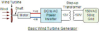
It is possible to use a 12V DC motor (I assume its a car starter motor) as a wind turbine generator to provide energy conversion between the mechanical torque from the wind rotor turbines, (called the prime mover) and the connected 150V load. A gearless two or three bladed upwind wind turbine using a permanent magnet DC motor can be used to charge a battery for energy storage through a rectifier and a typical wind turbine configuration is given as:

Generator Configuration

However, using a low voltage DC motor as a wind turbine generator is not always a good idea for the following reasons.
  • The DC motor may not be rated for continuous use and overheat.
  • The motors maximum rotational speed may be exceeded on a gusty day resulting in bearing or mechanical failure of the armature, slip-rings and brushes.
  • A DC motor used as a generator does not provide a constant output voltage, when the shaft speed and the load current vary.
  • The output current may be high at a low 12V DC voltage requiring large diameter, low resistance cables between the generator and batteries.
  • The storage batteries and inverter electronics need to be as close as possible to the generator to reduce power loss in the cables.
  • The motors permanent magnets will attract ferromagnetic dust and debris.
  • Also relating to your situation, a special centre tapped “step-up” transformer is required to convert the 12V to 150V.
  • Then the alternative is to use a high voltage output wound rotor induction machine as a Wind Power Generator.
Regarding the electronics. You need to increase the voltage from 12 volts to 150 volts, therefore you will need a step-up transformer with a turns ratio of 1:12.5, The output power required on the secondary winding is: V x I = 150 x 1.5 = 225 VA minimum. Then the primary winding will be: 225 ÷ 12 = 18.75 amps. Therefore, you will require a transformer with a primary winding capable of handling 20 amps minimum as well as the switching transistors.
For a 50 or 60Hz output frequency the primary switching transistors (or Mosfets) need to switch at this frequency. A simple RC or RL oscillator can be constructed to produce the required sinusoidal waveform to convert the DC to an AC signal. It must have two complementary outputs “Q” and “not Q” to switch both halves of the transformer primary, You can use NAND gates or NOT gates (7400, 7404, 4069 etc) as an IC multivibrator but these will produce a square wave output signal.
The switching transistors can be any high current type capable of switching 20 amps at 40 volts minimum such as the 2N3771 or the TIP35C, or use lower current transistors in parallel but use a heatsink. Darlington transistors such as the NPN 2N6284 or the NPN SGSD100. One suggested (but not tested) switching circuit could be:
Possible Switching Circuit


Each half of the transformer primary is switched in turn to produce the secondary output. Because of the high current flow in the primary windings large diameter cables must be used. The pilot switching transistors can be any small 5-6 amp NPN transistor such as the TIP41, TIP121 etc. The diode is a normal 1-2 amp power diode.


Design by Free WordPress Themes | Bloggerized by Lasantha - Premium Blogger Themes | cheap international calls