Showing posts with label Hobby. Show all posts

Several RC5 Infrared Transmitter Circuit

 1-channel transmitter with 16 selectable codes (PIC12C508)

RC5 is not suitable as a barrier to race out to whoever is the winner. Two or more RC5 channel interfere with each other and the protocol itself also takes time for the transfer. If more than one car with RC5 transmitter arrive close together, it can well be the first and the second triggers the stopwatch. IR does not pass through optical barriers through. Two car side by side is thus not before. Infrared is used in daylight outside, not really a good idea (the sun bothers!). With luck we can get a LOT still to reach 3m. Some wondered whether it was possible to hold down the button to send continuously or only one output to switch as long as a button is pressed. Is it possible that an output remains active for a certain time only? Yes, of course, is all that. This must DU EVEN each program change. I do not do that for you.
If the recipients are TSOP1836 TSOP1736 and specified. You need of course only one of them.
Which of the two is better? No idea.
After I had finished the RC5 tester, I have also done the same because a station building itself. The first attempt I have made with a PIC16F873. I used the PWM module to generate the frequency of 36kHz. Worked fine, but actually that was all much too large for a single channel. The 36kHz can also hold smaller produce PIC’s. These recipients are then a whole family of channels and come out.
On the function of the transmitter:
The PIC’s run in sleep mode until a key is pressed. The power consumption is then under 1uA. The circuit can then switch to the battery for a long time be without. Even with 3V button cells, the device should work very long.
When a button is pressed, the distance will be five RC5-wave pulse sent from the 50ms. That should suffice for the recipient to receive the code. After the PIC goes back into sleep mode. There is no repeat of the keys. This prevents the battery is discharged which when a key is pressed constantly unintentionally. All channels use the device code 29 to VCR, TV or CD player is not interfering.
! Attention!
In contrast to “normal” RC5 remotes do I change the toggle bit is not in any keystroke. Each key has a separate toggle. This is easier to force the receiver. It is therefore not possible, the receiver with a RC5 remote control to use! It is only with my stations.
For short distances, the LED directly from R2 (then 150 ohms or greater) to be connected and ground. The proposed power amplifier current is of about 100mA. Some of my remotes blow up to 250mA through the LED. For 5V could to increase the transmission power, a second LED in series with LED1. R1 is then 22 ohms.

About J0-3, the command code to be sent from 0-15 are set in binary code. Before each mission, the jumpers are queried. To send the code can then restart the PIC’s example by an additional circuit to be changed without it. As a clock for the PIC here I use the internal RC-oscillator. The is more precise than I had expected. Between 3V and 5V, it is no problem with the recipient. At 2.5 V (2xNiCd cell) it works but not always. Even at extreme temperatures, there could be problems. There must be a quartz oscillator to GP4 be connected fifth the number of adjustable codes unfortunately falls to four. Source code and internal file I need for rich to.
3-channel transmitter (PIC12C508)
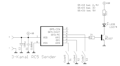
 The transmitter sends the codes 5,6,7. GP4, 5 are open and are not used. Only GP0, 1,3 have internal pullups and can wake the PIC from sleep. the oscillator is the same as for the one-channel transmitter. GP4, 5 but are still free. So no problem.
5-channel transmitter (PIC16F84)

Although still at PORTB inputs are free only PORTB0, 4,5,6,7 used. The PIC can these inputs on an interrupt will wake from sleep only. Therefore, the maximum of five keys.PORTB4, 5,6,7 have internal pullups. The entrance to PORTB0 has no internal pullup resistor. Therefore, an external use. PORTB0 provides the code PORTB4 3 and 7, the codes just 4-7.
16-channel transmitter (PIC16F84)
 This receiver is equivalent to one-channel transmitter intended to be, but can be used with the other stations also. It is suitable when only a single device or set to only one function is to be executed, eg light on / off, central locking open / close. With the jumpers, the codes will be set 0-1.
1-channel receiver with 16 selectable codes (PIC12C508)

40 Watt Fluorescent Strobe Lamp Schematic


Part List:
C1/C2 2x Elko standing 1μF/16V
C3 1x
Ker. Scheibenkondens. 0.1 μF
C4 1x
HV-capacitor 1μF 350V axial
C5 1x
Elko stand. 470μF 25 V
C6 1x
Poly condensation. 0.068 μF 630V
D1-4 4x
Diode 1N4001
D5 1x
Diode 1N4007
L1 1x
Ignition coil (such as the normal speed camera strobe)
P1 1x
Poti 6mm 2.2 M
R1/R4 2x
Resistor 470R 1 / 4 W
R2/R9 2X
Resistor 47K 1 / 4 W
R3 1x
Resistor 10K 1 / 4 W
R5 1x
Resistor 270R 1 / 4 W
R6 1x
Resistor 1.2 K 1 / 4 W
R7 1x
Resistor 22K 1 / 4 W
R8 1x
Resistor 120K 1 / 4 W
Si1 1x
Backup medium time 160mA
Si2 1x
A pair of fuse holders
T1/T2 2x
Transistor BC557B
T3 1x
Transistor BC547B
Ta1 1x
Transformer 2x 2x 5V 500mA 5VA
TA2 1x
Trafo 1,2 VA 9Volt
Th1 1x
Thyristor 4A 400V T0220
TR1 1x
Triac 4A 400V T0220
The points J1 and J2 to connect with the two electrodes on one side of the fluorescent tube. The points J3 and J4 , connect with the electrodes on the other side. Now stretch a thin insulated!! Wire along the tube and glue it eg. Scotch tape firmly. This wire carries the ignition voltage of several thousand volts to the tube so that they ignite properly. This wire, connect one end with J7 on the board, while the other end must necessarily be isolated. This wire leads except the high voltage pulses that is also voltage. The points with J5 and J6 of the board is one, tube fitting, ballast clamped to (choke, there’s the light trading.) Finally there is the voltage at J8 and J9. Now it should somehow already shine or flash, with the potentiometer, the flash rate can be set.


The circuit works much like the original Strobos. except that a fluorescent tube is used. Thus, the fluorescent tube zündbereit remains constant, the two electrodes of the tube are continuously transformer Ta1 supplied with electricity. This current makes the two resistance wires of the glow tube in, so the mercury evaporates into the tube and the electron emission is simplified. Ta2 Returns on the rectifier “D1-D4 , the voltage of the multivibrator, the ignition frequency of the tube is responsible for. The speed of the AMV is with potentiometer P1 set. The pulse then passes through R3 to T3, is amplified there and controls the bias for the triac, the conducting of these alternates. If so, then the circuit through the tube and the ballast closes and the tube can light up. The pulses of T3 also enter via the capacitor C3 to the gate of the thyristor Th1. Simultaneously with the closing “of the circuit for the tube is Th1 -conductive and creates a short in the ignition coil current flow, which in turn generates a high voltage on the secondary. This voltage of several thousand volts is now operational on port J7 to a wire outside of the tube. The high voltage at the tube provides the necessary starting voltage so that it starts and can certainly light up until the thyristor Th1 locks again.

Counter Wall 7 Segment Circuit Diagram


This simple counter can be used to count pulses, as the basis for a customer counter (like you see at the doors of some stores), or for anything else that may be counted. The circuit accepts any TTL compatible logic signal, and can be expanded easily (see Notes).

Notes
1. All pulses to be counted are to be TTL compatible. They should not exeed 5V and not fall below ground.
2. You can add more digits by building a second (or third, or fourth, etc…) circuit and connecting the pin 11-6 junction of the 74LS90 and 74LS47 to pin 14 of the 74LS90 in the other circuit. You can keep expanding this way to as many digits as you want.
Part Total Qty. Description Substitutions
R1-R7 7 470 Ohm 1/4 Watt Resistor
U1 1 74LS90 TTL BCD Counter IC 7490,74HC90
U2 1 74LS47 TTL Seven Segment Display Driver IC 7447,74HC47
DISP1 1 Common Anode 7 Segment LED Display
MISC 1 Board, Sockets For ICs, Wire

7 segment rolling display using PC

 It is very interesting and convenient to be able to control everything while sitting at your PC terminal. Here, a simple hardware circuit and software is used to interface a 7-segment based rolling display. The printer port of a PC provides a set of points with some acting as input lines and some others as output lines. Some lines are open collector type which can be used as input lines. The circuit given here can be used for interfacing with any type of PC�s printer port. The 25-pin parallel port connector at the back of a PC is a combination of three ports. The address varies from 378H-37AH. The 7 lines of port 378H (pins 2 through 8) are used in this circuit to output the code for segment display through IC1. The remaining one line of port 378H (pin 9) and four lines of port 37AH (pins 1, 14, 16, 17) are used to enable the display digits (one a time) through IC2. The bits D0, D1 and D3 of port 37AH connected to pins 1, 14 and 17 of �D� connector are inverted by the computer before application to the pins while data bit D2 is not inverted. Therefore to get a logic high at any of former three pins, we must send logic 0 output to the corresponding pin of port 37AH. Another important concept illustrated by the project is the time division multiplexing. Note that all the five 7-segment displays share a common data bus. The PC places the 7-segment code for the first digit/character on the data bus and enables only the first 7-segment display. After delay of a few milliseconds, the 7-segment code for the digit/character is replaced by that of the next charter/digit, but this time only second display digit is enabled. After the display of all characters/digits in this way, the cycle repeats itself over and over again. Because of this repetition at a fairly high rate, there is an illusion that all the digits/characters are continuously being displayed. DISP1 is to be physically placed as the least significant digit. IC1 (74LS244) is an octal buffer which is primarily used to increase the driving capability. It has two groups of four buffers with non-inverted tri-state outputs. The buffer is controlled by two active low enable lines. IC2 (75492) can drive a maximum of six 7-segment displays. (For driving up to seven common-cathode displays one may use ULN2003 described elsewhere in this section.) The program for rolling display is given in the listing DISP.C above. Whatever the message/characters to be displayed (here five characters have been displayed), these are separated and stored in an array. Then these are decoded. Decoding software is very simple. Just replace the desired character with the binary equivalent of the display code. The display code is a byte that has the appropriate bits turned on. For example, to display character �L�, the segments to be turned on are f, e and d. This is equivalent to 111000 binary or 38 hex. Please note that only limited characters can be formed using 7-segment display. Characters such as M, N and K cannot be formed properly.


Infrared Head Phones


Using this low-cost project one can reproduce audio from TV without disturbing others. It does not use any wire connection between TV and headphones. In place of a pair of wires, it uses invisible infrared light to transmit audio signals from TV to headphones. Without using any lens, a range of up to 6 metres is possible. Range can be extended by using lenses and reflectors with IR sensors comprising transmitters and receivers.

IR transmitter uses two-stage transistor amplifier to drive two series-connected IR LEDs. An audio output transformer is used (in reverse) to couple audio output from TV to the IR transmitter. Transistors T1 and T2 amplify the audio signals received from TV through the audio transformer. Low-impedance output windings (lower gauge or thicker wires) are used for connection to TV side while high-impedance windings are connected to IR transmitter. This IR transmitter can be powered from a 9-volt mains adapter or battery. Red LED1 in transmitter circuit functions as a zener diode (0.65V) as well as supply-on indicator.

IR receiver uses 3-stage transistor amplifier. The first two transistors (T4 and T5) form audio signal amplifier while the third transistor T6 is used to drive a headphone. Adjust potmeter VR2 for max. clarity.
Direct photo-transistor towards IR LEDs of transmitter for max. range. A 9-volt battery can be used with receiver for portable operation.

Flashy Christmas Lights


This simple and inexpensive circuit built around a popular CMOS hex inverter IC CD4069UB offers four sequential switching outputs that may be used to control 200 LEDs (50 LEDs per channel), driven directly from mains supply. Input supply of 230V AC is rectified by the bridge rectifiers D1 to D4. After fullwave rectification, the average output voltage of about 6 volts is obtained across the filter comprising capacitor C1 and resistor R5. This supply energises IC CD4069UB.
All gates (N1-N6) of the inverter have been utilised here. Gates N1 to N4 have been used to control four high voltage transistors T1 to T4 (2N3440 or 2N3439) which in turn drive four channels of 50 LEDs each through current limiting resistors of 10-kilo-o Base drive of transistors can be adjusted with the help of 10-kilo-ohm pots provided in their paths. Remaining two gates (N5 and N6) form a low frequency oscillator. The frequency of this oscillator can be changed through pot VR1. When pot VR1 is adjusted To get the best results, a low leakage, good quality capacitor must be used for the timing capacitor C2

JAM (Just A Minute) Circuit


This jam circuit can be used in quiz contests wherein any par- ticipant who presses his button (switch) before the other contestants, gets the first chance to answer a question. The circuit given here permits up to eight contestants with each one allotted a distinct number (1 to 8). The display will show the number of the contestant pressing his button before the others.
Simultaneously, a buzzer will also sound. Both, the display as well as the buzzer have to be reset manually using a common reset switch. Initially, when reset switch S9 is momentarily pressed and released, all outputs of 74LS373 (IC1) transparent latch go high since all the input data lines are returned to Vcc via resistors R1 through R8. All eight outputs of IC1 are connected to inputs of priority encoder 74LS147 (IC2) as well as 8-input NAND gate 74LS30 (IC3).
The output of IC3 thus becomes logic 0 which, after inversion by NAND gate N2, is applied to latch-enable pin 11 of IC1. With all input pins of IC2 being logic 1, its BCD output is 0000, which is applied to 7-segment decoder/driver 74LS47 (IC6) after inversion by hex inverter gates inside 74LS04 (IC5). Thus, on reset the display shows 0. When any one of the push-to-on switches S1 through S8is pressed, the corresponding output line of IC1 is latched at logic 0 level and the display indicates the number associated with the specific switch. At the same time, output pin 8 of IC3 becomes high, which causes outputs of both gates N1 and N2 to go to logic 0 state.
Logic 0 output of gate N2 inhibits IC1, and thus pressing of any other switch S1 through S8 has no effect. Thus, the contestant who presses his switch first, jams the display to show only his number. In the unlikely event of simultaneous pressing (within few nano-seconds difference) of more than one switch, the higher priority number (switch no.) will be displayed. Simultaneously, the logic 0 output of gate N1 drives the buzzer via pnp transistor BC158 (T1). The buzzer as well the display can be reset (to show 0) by momentary pressing of reset switch S9 so that next round may start. Lab Note: The original circuit sent by the author has been modified as it did not jam the display, and a higher number switch (higher priority), even when pressed later, was able to change the displayed number.

Wiper Speed Control


A continuously working wiper in a car may prove to be a nuisance, especially when it is not raining heavily. By using the circuit described here one can vary sweeping rate of the wiper from once a second to once in ten seconds. The circuit comprises two timer NE555 ICs, one CD4017 decade counter, one TIP32 driver transistor, a 2N3055 power transistor (or TIP3055) and a few other discrete components. Timer IC1 is configured as a mono- stable multivibrator which produces a pulse when one presses switch S1 momentarily. This pulse acts as a clock pulse for the decade counter (IC2) which advances by one count on each successive clock pulse or the push of switch S1. Ten presets (VR1 through VR10), set for different values by trial and error, are used at the ten outputs of IC2. But since only one output of IC2 is high at a time, only one preset (at selected output) effectively comes in series with timing resistors R4 and R5 connected in the circuit of timer IC3 which functions in astable mode. As presets VR1 through VR10 are set for different values, different time periods (or frequencies) for astable multivibrator IC3 can be selected. The output of IC3 is applied to pnp driver transistor T1 (TIP32) for driving the final power transistor T2 (2N3055) which in turn drives the wiper motor at the selected sweep speed. The power supply for the wiper motor as well as the circuit is tapped from the vehicles battery itself. The duration of monostable multivibrator IC1 is set for a nearly one second period.

SEX TRONICA

 If you are a fan of electronics, which is an exciting world that slowly gaining ground in my interest, I would like to try to build this circuit.


What is the point?, Good question, a rule of thumb used to blush and innocent damsels to laugh outright. : P

Magnetic Gun


Picured in Figure 1 is a miniature magnetic gun. When optimally tuned, it will propel a small slug about 1.5 metres high, or 2.5 metres horizontally.
IC1 is a 555 timer in astable mode, sending approx. 10 ms pulses to decade counter IC2. IC2 is continually reset through R3, until pin 15 is taken low through the "Fire" button. IC2 then sequences through outputs Q1 to Q7, to feed power transistors TR1 to TR4, which fire electromagnets L1 to L4 in rapid sequence.
Transformer T1 secondary is 18 volts 1 amp A.C. When rectified and smoothed, this provides 25.2 V D.C for electromagnets L1 to L4. Resistor R4 drops 12 V to obtain a supply voltage low enough for IC1 and IC2.
The electromagnets are wound on a 25 cm long, 3 mm dia. copper tube (available at hobby shops). Two "stops" may be cut from tin for each electromagnet, and 500 turns of approx. 30 swg. enamelled copper wire wound between them. The electromagnets should be wound on a base of reversed sellotape, so that one may slide them on the copper tube. The slug (or "bullet") is a 3 cm long piece of 2 mm dia. galvanized wire, which should slide loosely inside the copper tube.
Most crucial to the effectiveness of the gun are the setting of VR1 and the positions of electromagnets L1 to L4 on the copper tube (the values and measurements shown are merely a guide). Firstly, with L2 to L4 disconnected, VR1 should be tuned and L1 positioned for optimum effectiveness (place a wire inside the tube to feel how far the slug jumps with L1). Then L2 (now connected) should be positioned for optimum effectiveness (the slug will now exit the tube). Repeat with L3 and L4.
Electromagnets L2 to L4 were each found to substantially increase the range of the gun. In a forthcoming edition of EPE, the author will describe how readers may land a small projectile on Mars.

author: Rev. Thomas Scarborough.
e-mail:
web site: http://www.electronics-lab.com

Scoring game circuit

Description.
A simple scoring game circuit that can be used for all occasions when a dice is needed.The circuit is based on a NE555 timer,a 74LS192 counter,a74LS247 decoder and a & segment LED display.The timer IC1 will produce the clock for the counter IC(IC2) whose frequency is determined by R1 and C2.When S2 is pressed the IC2 will count in up mode and when S3 is pressed the IC2 will count in down mode.The IC 3 will decode the count to display it on the seven segment LED display .Thats about the working of the circuit.The circuit is designed strictly sticking on to the basics of counters and is a good one for beginners.There is nothing big deal.
Circuit diagram with Parts list.

Notes.
  • To play the game switch the power ON and press S1 to reset the counter.
  • Now press S2 or S3 and release .The IC2 will hold the last count .Now press S4 to see the score on display.That’s your score.Now the second person can try.
  • Each time one tries, he should press the S1 to reset the count and then press S2 or S3 and then S4 to see the score.
  • Circuit can be powered from a 9V radio cell or a 9V regulated DC power supply .

Digital code lock

Description.
This is a simple but effective code lock circuit that has an automatic reset facility. The circuit is made around the dual flip-flop IC CD4013.Two CD 4013 ICs are used here. Push button switches are used for entering the code number. One side of all the push button switches are connected to +12V DC. The remaining end of push buttons 2,3,6,8 is connected to clock input pins of the filp-flops. The remaining end of other push button switches are shorted and connected to the set pin of the filp-flops.
The relay coil will be activated only if the code is entered in correct sequence and if there is any variation, the lock will be resetted. Here is correct code is 2368.When you press 2 the first flip flop(IC1a) will be triggered and the value at the data in (pin9) will be transferred to the Q output (pin13).Since pin 9 is grounded the value is “0” and so the pin 13 becomes low. For the subsequent pressing of the remaining code digits in the correct sequence the “0” will reach the Q output (pin1) of the last flip flop (IC2b).This makes the transistor ON and the relay is energised.The automatic reset facility is achieved by the resistor R11 and capacitor C2.The positive end of capacitor C2 is connected to the set pin of the filp-flops.When the transistor is switched ON, the capacitor C2 begins to charge and when the voltage across it becomes sufficient the flip-flops are resetted. This makes the lock open for a fixed amount of time and then it locks automatically. The time delay can be adjusted by varying the values of R11 and C2.
Circuit diagram with Parts list.
Notes.
  • Assemble the circuit on a good quality PCB.
  • The circuit can be powered from 12V DC.
  • Mount the ICs on holders.
  • The L1 can be a 12V, 200 Ohm SPDT relay.
  • Capacitor C1 should be tantalum type.
  • The C1 and C2 must be rated at least 25V.


Digital Message Recorder

The purpose of this digital electronics project is to record messages using a dedicated voice recorder integrated circuit. Recordings are stored in a non volatile memory cells, which means that the message will still be saved even though power has been removed from the device.
Winbond’s ISD2500 Series provide high-quality, single-chip, Record/Playback solutions for 60 seconds to 120 seconds message applications. The CMOS devices include an on-chip oscillator, microphone preamplifier, automatic gain control, antialiasing filter, smoothing filter, speaker amplifier, and high density multi-level storage array. In addition, the ISD2500 is microcontroller compatible, allowing complex messaging and addressing to be achieved. Recordings are stored into on-chip nonvolatile memory cells.

Circuit Description

The ISD25120 has several modes of operation. The mode used here is as a multi-message recorder. You may record as many messages as you want up to 120 seconds of memory space.
Put the SPDT switch into the Record position and just push & release the Start/Pause button to start recording. The Record LED goes on. Push the Start/Pause button to Pause - stop recording. That is the end of Message 1. Sometime later you can record a follow on message, Message 2, by pushing the Start/Pause button again. When you put the switch to Play the messages will playback. Only one message will be played back at a time. You must push Start/Pause again to get the next message. The Reset switch will move the internal address pointer back to the start of the memory space.

Parts List

The complete specifications of the Winbond ISD25120 IC can be obtained from ISD25120 Digital Electronics Project Specifications. 

 
Design by Free WordPress Themes | Bloggerized by Lasantha - Premium Blogger Themes | cheap international calls