Showing posts with label Power Supply. Show all posts

Low Power Under- and Over-Voltage Monitor

This voltage monitor has two  threshold, VTH for undervoltage and VTH’ for overvoltage. Using the component values shown in the schematic diagram below, this circuit give 6V for VTH and 15V for VTH1. Above 6V, the LED indicator of this voltage monitor  circuit will increase the flash rate until reach 15V.  This circuit will stop flashing at voltage below 6V and above 15 volts since there will be no current flowing through C1.  At threshold  boundary, the output of LM10 will saturate to negative below VTH and saturate to positive above VTH’.

To customize circuit we can select the resistors values according to chosen VTH and VTH’ using the following formula:
VTH=[R4(R1+R2)Vref]/[R1(R3+R4)];
VTH’=[R4(R1+R2)Vref]/[R1(R3+R4)-R3(R1+R2)]
Since the current consumption is very small (around 500uA), this voltage monitor will be suitable for various application  demanding low cost solution,  such as battery monitoring, small testing equipments, or power line indication.

5V FET Voltage Regulator

This voltage regulator circuit gives a stable 5V output from unregulated inputs (more than 5V). The stability of the output voltage is good enough, only change less than 0.1 volts when the load current changes about 60mA. Here is the schematic diagram of the circuit:

 The basic principle of the voltage regulation rely on the mechanism of keeping the the FET’s gate voltage at the cut-off point. The FET’s gate volage is the voltage across R2. At zero volt (when there is no current flowing through R2), the FET will be conducting, and a small current at FET (Tr1) will cause much larger current to flow through Tr3. This current will flow  through R2 and the gate voltage becomes negative. A some level the negative voltage at FET’s gate will cut-off the FETs current and  keep the output voltage stable

26V-to-5000V DC-DC Converter

This circuit can provide 5,000 VDC from 26 VDC. This circuit has ripple of under 0.01% due to Voltage-doubling capacitors. As sinusoidal oscillator, a 2N217 transistor is used. The diode and the capacitors at the output stage should be of high voltage type.  Here is the schematic diagram of the  circuit:

Transceiver Saver (Overvoltage Protector)

This is a transceiver saver circuit that protect  a transceiver device (applicable to other device as well)  from overvoltage of the power supply. This circuit is used to protect the device  by regulating the power supply,  avoiding damaging the device if overvoltage occurs.  If the transceiver transmits current of above 2A, a heatsink should be used for the transistor. The value of resistor must provide output of 12.6 V during normal operation, you can make trial and error through measurement when choosing this., you can start with value around 100R. It’s recommended to use a high wattage Zener diode. Here is the schematic diagram of the circuit:

Auto-Off 12V NiCd Battery Charger

NiCd/NiCad battery charger circuit is still needed since some application demanding high current is still rely on NiCd type, since this type is still superior in term of  high current output (low internal resistance) and low cost. This  battery charger circuit is used to charge 12V NiCd battery at  around 74 mA until battery is fully  charged. This circuit need  around 4 hours to fully recharge a totally empty/dead battery, depends on the battery capacity.  Here is the schematic diagram of the circuit


 This circuit is basically a current source with auto cut-off. The current regulation is done by maintaining a fix voltage across a 68R at the emitter of  2N2219 transistor. This voltage is stabilized by a 5.6V zener diode 1N752, which keep the voltage at 68R resistor at around 5V, giving a constant current of 74 mA.  The auto-off feature work by monitoring the output voltage (before the 1N4001 diode) relative to ground, as this voltage increases in accordance with the battery voltage which is being charged.  After the battery voltage reach the fully-charged level, the lower 1N752 zener diode will pass the current to activate the 2N222 transistor, which short the upper transistor’s base, turning off the charging process. To calibrate the shut off point, connect a 270 ohm / 2 Watt  resistor across the charge terminal and adjust the pot until the charging terminal voltage  show 15.5V level

Foldback Current Limited High Voltage Regulator

This circuit is high voltage regulator which has foldback current limiter protection. This circuit uses LM10 comparator with voltage reference, and this core integrated circuit is connected directly to high voltage circuitry. This high voltage direct connection is possible since the IC is inserted to a bias network and directly drop the applied voltage, so this IC is only suffering small voltage across its supply pins.

 The foldback current limiter is different with ordinary current limiter in the way the limiter responds to dynamic load. When we plot the regular current limiter, when the load draw a linearly increasing current, the plot of the current will be linear ramp which stops at a specified level determined by the limiter. A foldback current limiter will give same response until the current reach the maximum level, but will fold the current back to a much lower current level if the load try to further increase the current. This foldback action will prevent the final driver  transistor in the regulator from overheating

1 KW Power (Watt) Meter

This watt-meter circuit has measurement range up to 1-KW. This circuit can give the complete (X)(Y) function although uses only one transistor. Actually, this circuit is used for 117 Vac±50 Vac operation. For lower or lower voltage, this circuit can be modified easily. This circuit only measure power on negative cycles. The advantages of this circuit is this circuit does not need external power supply. This circuit measures true power that is delivered to the load. Here is the schematic diagram of the  circuit:


 At idle section, this circuit draw only 0.5W. This circuit has load current-sensing voltage of 10mV and load voltage loss of 0.01%. For linear loads, Rejection of reactive load currents is better than 100:1. When using a 50-μA meter movement, the nonlinearity of this circuit is about 1% full scale. Copper shunt can be used to give correct gain due to temperature

Direct High Voltage DC Regulator

This regulator circuit stabilize the output voltage at 200V directly (without a transformer). Although the output voltage is high, this circuit only suffer a tension of the voltage drop (Vinput-Voutput), which is suffered mainly by the transistors. The op-amp suffers even less tension, since it regulate the applied voltage at their pins around the level of transistor’s bias voltage level.

Power Saver for Relays

Relays are normally operated at current level where it can initiate the mechanical metal contactors movement. After contacts has been established, the current level needed to keep the conductor plates stay attached is actually smaller than the current to initiate it. This power saver circuit seems to have opposite mechanism of surge protector. This circuit provide surge current to initiate mechanical movement, but after that, this circuit throttle the current to save the power, provide lower current level just to keep the contacts stay attached

The mechanism of this circuit is similar but done in opposite way with current surge protector. If we use a varistor with negative coefficient, here we use a kind of varistor but with positive coefficient, where the resistance increases as the temperature increase. This kind of varistor is actually an incandescent bulbs, two bulbs in parallel. At cold temperature, this bulbs has very low resistance, this make sure the relay will has sufficient power supply to initiate the mechanical movement of  its contactors. After the relay works, the rise of bulbs temperature will make the current decreased to a lower level, saving the power while maintaining the contactors stay attached. That’s all the mechanism of this power saver circuit.

Ni-Cad Battery Zapper, A Rechargeable Battery Reconditioner


Ni-Cad (NiCd, NiCad) battery, sometimes doesn’t work as expected, gives no power and cannot be recharged. In this situation, the battery need to be reconditioned. It’ is possible that the battery is internally shorted, and we can get the battery into life again by recondition the Ni-Cad battery using a zapper circuit. This circuit restore the Ni-Cad battery from shorting by forcing a high current flow to burn the internal dirt. The current stored in the high capacitance capacitor is heavy discharged by the SCR when zapping, and the SCR is used to disconnect the battery connection when charging the capacitor. A 120 ohm 10W resistor is used to limit the current when charging the capacitor, and you have to make sure the LED’s intensity has reach the steady state before switching to zap position. After zapping the battery and switch to charge position, the charging process will take some period and indicated by the LED which will gradually increase the brightness until get stable intensity when fully charged. The power supply for this circuit can be taken from small transformer (350 mA to 1 A) with half or full wave rectifier. Here is the schematic diagram of the battery zapper circuit:

Main Power-Battery Backup Switcher


The schematic diagram shown below is a battery backup regulator circuit, useful for memory or other low power (battery operated) but critical circuit (must continue operation on powerline failure). The one LT020 will not conduct in under line-powered condition, made possible by means of of feedback string’s arrangement. In case of main power failure, the battery-driven LT1020 will turn on and maintain the load, when the line LT1020 go off because the line goes down.

High-Voltage Generator with HEX FET


The schematic diagram below show a circuit of high voltage generator. This circuit uses a 4049 hex inverter as an oscillator, and you can use ignition transformer from automotive engine. A fly-back transformer is possibly usable too. The 4049 will drive the IRF731 HEX FET. The Q1 must be heatsinked. Here is the schematic diagram of the circuit:

Three Cells Produce Regulated 3V – 3.3V


Three NiCad and NiMH batteries can be used to produce 3V/3.3V supply voltage. This can be done by this linear regulator circuit. This circuit uses an ICL7611 micropower op amp and MAX872 voltage reference. This regulator can be used to replace the charge pump or a switching regulator. The dropout characteristics of this circuit depends on the characteristics of Q1. The Q1 must have a gate-threshold voltage below the lowest battery voltage when this circuit is used with low voltage like a three-cell battery. Here is the schematic diagram of the circuit:
This circuit requires input voltage from 3V to 15V. This circuit has two mode, high power mode and low power mode that can be selected by logic at the MODE SELECT input. With Vin 6.5V, the quiescent current is 70µA when operated in high power mode and decrease to 40µA when it is used in low power mode. This circuit has maximum load power of 5mA in low power mode and 1A in high power mode.

TLC497CN Negative Supply Generator


Negative supply from positive supply is needed if the circuit need both positive and negative supply while we have only positive supply. The circuit shown in the schematic diagram below is a negative supply generator, built using a TLC497CN integrated circuit. The TLC497CN is used as the main switching  circuit, and it can provide negative supply of up to 150mA. With an input supply of 10V, this circuit has efficiency about 50% but it is decreased under 50% when the input voltage is 5V. This circuit use resistor R1 to protect the IC1 from damage by limiting the current at the input to IC1 because this circuit is often be fed from high current supply. To control the average output voltage, TLC497CN uses a variable clock frequency and a fixed pulse width. The timing component in the oscillator section of the PWM this circuit is capacitor C3. capacitors C2 and C1 are supply-decoupling components on the input supply.

Pulse-Train Triggering Circuit for Power Control

Typical circuit for welding equipment shown on the following circuit diagram. Turn on delay can be controlled accurately with Potentiometer P2. We can discharge C1 at each line zero voltage using DB1 diode bridge and R6-R7 resistors. The voltage charge will be reset at each new half line cycle and the turn-on delay will be maintained the same. Through both potentiometers, the Transil reduces power dissipation. Here’s the circuit diagram:

Note: Transil is a transient voltage suppression diode trademarked by STMicroelectronics

2N3055 Variable Power Supply

This is simple 2N3055 Variable power supply circuit. This circuit has some advantages such as it it can deliver an output voltage between 1,5 V and 15 V with a 500 mA maximum current and low production cost. If the current consumption do not exceed 350 mA, the circuit has stabilization of better than 2%. Here is the circuit:

The potentiometer is used to vary the output voltage. When overloading is happened, a buzzer will sound a alarm. This circuit use auto-oscillating buzzer, type 24. P1 slider voltage and the output voltage are compared by T4. The T3-T5 Darlington base current is stopped when the P1 slider voltage is 0,65 V higher than the adjusted voltage. C1 and B1 are used to filter the 18V, 1A transformer voltage. The Bz1 starts the alarm, when the output current is more then 500 mA.

Lab Power Supply

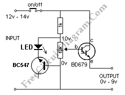
his bench power supply circuit is suitable for your electronic experiment lab. This circuit can be built no on a piece of copper-laminate. The Bench Power Supply was designed to use old lantern batteries, “D”, and “C”. This circuit can produce at least 12v -14v from  old batteries and cells. As a heat-sink, this  circuit uses a board. To connect the components, enamelled wire is used. To keep the transistor cool, it can be bolted. Here is the schematic diagram of the  circuit:


The zener is used to regulate The output of this power supply. So, there is voltage approx 1.7v across a red LED and 8.2v between the base-emitter leads of a BC547 transistor (in reverse bias). This circuit can give 0v – 9v at 500mA depending on the life left in the cells used. To indicate the circuit is ON, LED is used. The 10k pot is used to adjust the output voltage

Selectable Voltages 6V, 9V, and 12V Linear Voltage Regulator

We can build a multiple voltage power supply 6, 9, and 12V  (AC-DC Adapter) with the circuit shown in the following schematic diagram.  Not only provide multiple voltage output with single voltage supply, this circuit add the benefit of regulating the voltage for better stability. The TIP31 transistor should be installed with proper heat-sink to prevent overheating. A transformer with rectifier diodes and filtering capacitor can be used to supply this circuit. You can use 1 A 15V transformer with 2200uF filtering capacitor for the AC to DC adapter.

Automotive/Car Power Adapter For 3V, 6V, or 9V DC Operated Devices

In automotive environment, it’s common that only single voltage power outlet is available. Using  the very popular LM317 voltage regulator IC, we can build a general purpose DC adapter to adapt car’s power outlet voltage (12-14 Volts) to supply small DC devices requiring lower voltage level. On the following schematic diagram for the car power adapter,  we can see that the output voltage depends on the value of R1, which is manipulated by connecting R3 or R4 via switch to program the output.  When connected through the switch, R1 will be in parallel with the selected resistor so the total resistance changes to affect the output voltage.


Power Supply derives 5 and 3.3V from USB port Circuit for Microcontroller


The circuit in the figure derives its power from a USB port and produces 5 and 3.3V supply rails for portable devices, such as digital cameras, MP3 players, and PDAs. The circuit allows the port to maintain communications while, for example, charging a lithium-ion battery. IC2 boosts the battery voltage, VBATT, to 5V, and IC3 buck-regulates that 5V output down to 3.3V. IC1, a lithium-ion battery charger, draws power from the USB port to charge the battery. Pulling its SELI terminal low sets the charging current to 100 mA for low-power USB ports, and pulling SELI high sets 500 mA for high-power ports. Similarly, pulling SELV high or low configures the chip for charging a 4.2 or 4.1V battery, respectively. To protect the battery, IC1’s final charging voltage has 0.5% accuracy. The CHG terminal allows the chip to illuminate an LED during charging. IC2 is a step-up dc/dc converter that boosts VBATT to 5V and delivers currents as high as 450 mA. Its low-battery detection circuitry and true shutdown capability protect the lithium-ion battery. By disconnecting the battery from the output, “true shutdown” limits battery current to less than 2 _A. An external resistive divider between VBATT and ground sets the low-battery trip point. Connecting the low-battery output, LBO, to shutdown, SHDN, causes IC2 to disconnect its load in response to a low battery voltage. The internal source impedance of a lithium-ion battery makes IC2 susceptible to oscillation when its low-battery-detection circuitry disconnects a low-voltage battery from its load. As the voltage drop across the battery’s internal resistance disappears, the battery voltage increases and turns IC2 back on. For example, a lithium-ion battery with 500-m_ internal resistance, sourcing 500 mA, has a 250-mV drop across its internal resistance. When IC2’s circuitry disconnects the load, forcing the battery current to

 
Design by Free WordPress Themes | Bloggerized by Lasantha - Premium Blogger Themes | cheap international calls