Showing posts with label Telephones. Show all posts

Format Short Message Service

At command for communications with SMS-CENTER.
At hand phone GSM there is facility to data access applies serial connection, for data access is required by instruction sequence at interface hand phone. ETSI (European Telecommunication Standard Institute) that is the instruction standard in technical specification GSM. instruction phone is started with character AT and terminated with enter or 0Dh. Command received will be response with receiving of data ‘OK’ or ‘ Errors’. Applying AT Command important for SMS is:
AT+CMGS : to send SMS
AT+CMGL : to verify SMS
AT+CMGD : to vanish SMS
AT COMMAND for SMS usually followed by I/O started by units PDU. Streaming data or from SMS-CENTER must be in the form of PDU (Protocol Data Unit). PDU contains hexadecimal number what express language I/O. PDU consisted of some Header. Header to send SMS to SMS-CENTER differs from SMS received from SMS-CENTER. PDU send SMS to SMS-CENTER. There is eight header to send SMS, that is:
1. Number SMS CENTER
This first header divided to become three sub header
a. Number of couples hexa decimal SMS-CENTER in number hexa.
b. International Code and national code, header for national it is 81 and international is 91.
c. Number SMS-CENTER itself in couple hexa is turned over repeatedly.
example:
if number SMS-CENTER 0875400000
hence, writing national.
for writing of Heksa from SMS-CENTER 0875400000 becoming –>
80-57-04-00-00
so that writing as complete this is:
06818057040000 ==> value 06 showing there is 6 value tide
that is Code National(1 tide) + number SMS-CENTER(5 tide).
writing international
for writing of Hexsa from SMS-CENTER 62875400000 becoming –>
26-78-45-00-00-F0
so that writing as complete his is:
07912678450000F0 ==> value 07 showing there is 7 tide value that is Code International(1 tide) + number SMS-CENTER(6 tide).
2. Type SMS
Type AS OF neodymium SMS : 1 thus its a hexsa number is 01.
3. Number Reference SMS
Reference number gives value 0, causing the heksa value 00. Because later automatically will be given value by SMS-GATEWAY
4. Number Phone Acceptor
Writing of PDU at writing of phone number as follows:
a. Number of number decimal phone numbers gone to in number hexsa.
b. National or international Code. For National with code: 81. And international with code: 91
c. Number phone gone to in couple heksa is turned over repeatedly.
Example:
If phone number gone to be 081227153432.
For National Code :
at number gone to National is 081227153432 ==> the numbers 12 numbers ==> value hexsa 0C, and couple heksa from phone number gone to 80-21-72-51-43-23, hence writing is : 0C81802172514323
For International Code:
at number gone to International is 6281227153432 ==> number of numbers there are 13 numbers ==> value heksa 0D, and couple hexsa from phone number gone to 26-18-22-17-35-34-F2, hence writing it is : 0D91261822173534F2
5. form of SMS
0 ==> 00 –> SMS is sent in the form of SMS.
1 ==> 01 –> SMS is sent in the form of telex.
2 ==> 02 –> SMS is sent in the form of fax.
6.Scheme Encoding Data I/o
This time there are many the SMS Gateway in marketing applies 7 bit so that we apply code : 00, if there are still SMS Gateway which applies code bigger than 0 changed to Hexsa.
7. Duration Before SMS EXPIRED
If part of this skip, meant we are to derestricted time implementation of SMS.
8. Contents Of SMS
at part contents of SMS there are two sub Header.
a. Bulk length or number of contents of SMS
for example: to say ” Hi..” ==> there is 5 letter –> 05
b. Contents of in the form of number pair heksa phone or SMS-GATEWAY is having scheme encoding 7 bit to mean if we are etic a letter from key pad we make 7 successive I/O number, applies convertion ASCII to Heksa can. Or applies convertion itself that is:
first step : changes it becomes code 7 bit.
second step : changes code 7 bit to become 8 bit, what represented by couple hexsa.
so conclusion from writing of this PDU by writing down all sequences as follows :
Number SMS-CENTER – Type SMS – Reference number SMS – Number phone acceptor – Form Of SMS – Scheme Encoding Data I/O – duration before SMS expired – Contents Of SMS

Telephone Number Display


The given circuit, when connected in parallel to a telephone, dis- plays the number dialled from the telephone set using the DTMF mode. This circuit can also show the number dialled from the phone of the called party. This is particularly helpful for receiving any number over the phone lines. The DTMF signal 'generated by the phone on dialling a number' is decoded by DTMF decoder CM8870P1 (IC1), which converts the received DTMF signal into its equivalent BCD number that corresponds to the dialled number. This binary number is stored sequentially in 10 latches each time a number is dialled from the phone. The first number is stored in IC5A (1/2 of CD4508) while the second number is stored in IC5B and so on. The binary output from IC1 for digit '0' as decoded by IC1 is 10102 (=1010), and this cannot be displayed by the seven-segment decoder, IC10. Therefore the binary output of IC1 is passed through a logic-circuit which converts an input of '10102' into '00002' without affecting the inputs '1' through '9'. This is accomplished by gates N13 through N15 (IC11) and N1 (IC12). The storing of numbers in respective latches is done by IC2 (4017). The data valid output from pin 15 of IC1 is used to clock IC2. The ten outputs of IC2 are sequentially connected to the store and clear inputs of all the latches, except the last one, where the clear input is tied to ground. When an output pin of IC2 is high, the corresponding latch is cleared of previous data and kept ready for storing new data. Then, on clocking IC2, the same pin becomes low and the data present at the inputs of that latch at that instant gets stored and the next latch is cleared and kept ready. The similar input and output pins of all latches are connected together to form two separate input and output buses. There is only one 7-segment decoder/driver IC10 for all the ten displays. This not only reduces size and cost but reduces power requirement too. The output from a latch is available only when its disable pins (3 and 15) are brought low. This is done by IC3, IC12 and IC13. IC3 is clocked by an astable multivibrator IC4 (555). IC3 also drives the displays by switching corresponding transistors. When a latch is enabled, its corresponding display is turned on and the content of that latch, after decoding by IC10, gets displayed in the corresponding display. 

For instance, contents of IC5A are displayed on display "DIS1", that of IC5B on "DIS2" and so on. The system should be connected to the telephone lines via a DPDT switch (not shown) for manual switching, otherwise any circuit capable of sensing handset's off-hook condition and thereby switching relays, etc. can be used for automatic switching. The power-supply switch can also be replaced then. Though this circuit is capable of showing a maximum of ten digits, one can reduce the display digits as required. For doing this, connect the reset pin of IC2, say, for a 7-digit display, with S6 output at pin 5. The present circuit can be built on a veroboard and housed in a suitable box. The displays are common-cathode type. To make the system compact, small, 7-segment displays can be used but with some extra cost. Also, different colour displays can be used for the first three or four digits to separate the exchange code/STD code, etc. The circuit can be suitably adopted for calling-line display

Multipurpose Circuit for telephone


This add-on device for telephones can be connected in parallel to the telephone instrument.
The circuit provides audio-visual indication of on-hook, off-hook, and ringing modes. It can also be used to connect the telephone to a cid (caller identification device) through a relay and also to indicate tapping or misuse of telephone lines by sounding a buzzer.
 
In on-hook mode, 48V dc supply is maintained across the telephone lines. In this case, the bi-colour led glows in green, indicating the idle state of the telephone. The value of resistor r1 can be changed somewhat to adjust the led glow, without loading the telephone lines (by trial and error).

In on-hook mode of the hand-set, potentiometer vr1 is so adjusted that base of t1 (bc547) is forward biased, which, in turn, cuts off transistor t2 (bc108). While adjusting potmeter vr1, ensure that the led glows only in green and not in red.
When the hand-set is lifted, the voltage drops to around 12V dc. When this happens, the voltage across transistor t1's base-emitter junction falls below its conduction level to cut it off. As a result transistor pair t2-t3 starts oscillating and the piezo-buzzer starts beeping (with switch s1 in on position). At the same time, the bi-colour led glows in red.

In ringing mode, the bi-colour led flashes in green in synchronisation with the telephone ring.
A cid can be connected using a relay. The relay driver transistor can be connected via point a as shown in the circuit. To use the circuit for warning against misuse, switch s1 can be left in on position to activate the piezo-buzzer when anyone tries to tap the telephone line. (When the telephone line is tapped, it's like the off-hook mode of the telephone hand-set.)

Two 1.5V pencil cells can provide Vcc1 power supply, while a separate power supply for Vcc2 is recommended to avoid draining the battery. However, a single 6-volt supply source can be used in conjunction with a 3.3V zener diode to cater to both Vcc2 and Vcc1 supplies

Having secrecy in parallel telephones


Often a need arises for connection of two telephone instruments in parallel to one line. But it creates quite a few problems in their proper performance, such as overloading and overhearing of the conversation by an undesired person. In order to eliminate all such problems and get a clear reception, a simple scheme is presented here (Fig. 1).

This system will enable the incoming ring to be heard at both the ends. The DPDT switch, installed with each of the parallel telephones, connects you to the line in one position of the switch and disconnects you in the other position of the switch. At any one time, only one telephone is connected to the line. To receive a call at an end where the instrument is not connected to the line, you just have to flip the toggle switch at your end to receive the call, and act as usual to have a conversation. As soon as the position of the toggle switch is changed, the line gets transferred to the other telephone instrument.

Mount one DPDT toggle switch, one telephone ringer, and one telephone terminal box on two wooden electrical switchboards, as shown in Fig. 3. Interconnect the boards using a 4-pair telephone cable as per Fig. 1. The system is ready to use. Ensure that the two lower leads of switch S2 are connected to switch S1 after reversal, as shown in the figure.

Telephone call meter using calculator and COB


In this circuit, a simple calculator, in conjunction with a COB (chip-on-board) from an analogue quartz clock, is used to make a telephone call meter. The calculator enables conversion of STD/ISD calls to local call equivalents and always displays current local call-meter reading.
The circuit is simple and presents an elegant look, with feather-touch operation. It consumes very low current and is fully battery operated. The batteries used last more than a year.
Another advantage of using this circuit is that it is compatible with any type of pulse rate format, i.e. pulse rate in whole number, or whole number with decimal value. Recently, the telephone department announced changes in pulse rate format, which included pulse rate in whole number plus decimal value. In such a case, this circuit proves very handy.

To convert STD/ISD calls to local calls, this circuit needs accurate 1Hz clock pulses, generated by clock COB. This COB is found inside analogue quartz wall clocks or time-piece mechanisms. It consists of IC, chip capacitors, and crystal that one can retrieve from scrap quartz clock mechanisms. These can be purchased from watch-repairing shops for less than Rs 20.
Normally, the COB inside clock mechanism will be in good condition. However, before using the COB, please check its serviceability by applying 1.5V DC across terminals C and D, as shown in the figure. Then check DC voltage across terminals A and B; these terminals in a clock are connected to a coil. If the COB is in good condition, the multimeter needle would deflect forward and backward once every second. In fact, 0.5Hz clock is available at terminals A and B, with a phase difference of 90o. The advantage of using this COB is that it works on a 1.5V DC source.
The clock pulses available from terminal A and B are combined using a bridge, comprising diodes D1 to D4, to obtain 1Hz clock pulses. These clock pulses are applied to the base of transistor T1. The collector and emitter of transistor T1 are connected across calculator's '=' terminals.

The number of pulses forming an equivalent call may be determined from the latest telephone directory. However, the pulse rate (PR) found in the directory cannot be used directly in this circuit. For compatibility with this circuit, the pulse rate applicable for a particular place/distance, based on time of the day/holidays, is converted to pulse rate equivalent (PRE) using the formula PRE = 1/PR.
You may prepare a look-up table for various pulse rates and their equivalents (see Table). Suppose you are going to make an STD call in pulse rate 4. Note down from the table the pulse rate equivalent for pulse rate 4, which is 0.25. Please note that on maturity of a call in the telephone exchange, the exchange call meter immediately advances to one call and it will be further incremented according to pulse rate. So one call should always be included before counting the calls.

For making call in pulse rate 4, slide switch S1 to off (pulse set position) and press calculator buttons in the following order: 1, +, 0.25, =. Here, 1 is initial count, and 0.25 is PRE. Now calculator displays 1.025. This call meter is now ready to count. Now make the call, and as soon as the call matures, immediately slide switch S1 to on (start/standby position). The COB starts generating clock pulses of 1 Hz. Transistor T1 conducts once every second, and thus '=' button in calculator is activated electronically once every second. The calculator display
starts from 1.25, advancing every second as follows:
1.25, 1.5, 1.75, 2.00, 2.25, 2.50, and so on.
After finishing the call, immediately slide switch S1 to 'off' position (pulse set position) and note down the local call meter reading from the calculator display. If decimal value is more than or equal to 0.9, add another call to the whole number value. If decimal value is less than 0.9, neglect decimal value and note down only whole numbers.

To store this local call meter reading into calculator memory, press 'M+' button. Now local call meter reading is stored in memory and is added to the previous local call meter reading. For continuous display of current local call meter reading, press 'MRC' button and slide switch S1 to 'on' (start/standby position). The current local call meter reading will blink once every second.
In prototype circuit, the author used TAKSUN calculator that costs around Rs 80. The display height was 1 cm. In this calculator, he substituted the two button-type batteries with two externally connected 1.5V R6 type batteries to run the calculator for more than an year.

The power off button terminals were made dummy by affixing cellotape on contacts to avoid erasing of memory, should someone accidentally press the power 'off' button. This calculator has auto off facility. Therefore, some button needs to be pressed frequently to keep the calculator on. So, in the idle condition, the '=' button is activated electronically once every second by transistor T1, to keep the calculator continuously on.

Useful hints. Solder the '=' button terminals by drilling small holes in its vicinity on PCB pattern using thin copper wire and solder it neatly, such that the '=' button could get activated electronically as well as manually. Take the copper wire through a hole to the backside of the PCB, from where it is taken out of the calculator as terminals G and H.

At calculator's battery terminals, solder two wires to '+' and terminals. These wires are also taken out from calculator as terminals E and F. Affix COB on a general-purpose PCB and solder the remaining components neatly. For giving the unit an elegant look, purchase a jewellery plastic box with flip-type cover (size 15cm x 15cm). Now fix the board, calculator, and batteries, along with holder inside the jewellery box. Then mount the box on the wall and paste the look-up table inside the box cover in such a way that on opening the box, it is visible on left side of the box.
Caution. The negative terminals of battery A and battery B are to be kept isolated from each other for proper operation of this circuit.
LookUp Table
Pulse rate (PR)
2
2.5
3
4
6
8
12
16
24
32
36
48
Pulse rate eqlt. (PRE)
0.5000
0.4000
0.333
0.250
0.166
0.125
0.083
0.062
0.041
0.031
0.027
0.020
Note : Here PRE is shown up to three decimal places. In practice, one may use up to five or six decimal places.

Telephone line based audio muting and light on circuit


 Very often when enjoying music or watching TV at high audio level, we may not be able to hear a telephone ring and thus miss an important incoming phone call. To overcome this situation, the circuit presented here can be used. The circuit would automatically light a bulb on arrival of a telephone ring and simultaneously mute the music system/TV audio for the duration the telephone handset is off-hook. Lighting of the bulb would not only indicate an incoming call but also help in locating the telephone during darkness.

On arrival of a ring, or when the handset is off-hook, the inbuilt transistor of IC1 (opto-coupler) conducts and capacitor C1 gets charged and, in turn, transistor T1 gets forward biased. As a result, transistor T1 conducts, causing energisation of relays RL1, RL2, and RL3. Diode D1 connected in anti-parallel to inbuilt diode of IC1, in shunt with resistor R1, provides an easy path for AC current and helps in limiting the voltage across inbuilt diode to a safe value during the ringing. (The RMS value of ring voltage lies between 70 and 90 volts RMS.) 
Capacitor C1 maintains necessary voltage for continuously forward biasing  transistor T1 so that the relays are not energised during the negative half cycles and off-period of ring signal. Once the handset is picked up, the relays will still remain energised because of low-impedance DC path available (via cradle switch and handset) for the in-built diode of IC1. After completion of call when handset is placed back on its cradle, the low-impedance path through handset is no more available and thus relays RL1 through RL3 are deactivated.

As shown in the figure, the energised relay RL1 switches on the light, while energisation of relay RL2 causes the path of TV speaker lead to be opened. (For dual-speaker TV, replace relay RL2 with a DPDT relay of 6V, 200 ohm.) Similarly, energisation of DPDT relay RL3 opens the leads going to the speakers and thus mutes both audio speakers. Use NC' contacts of relay RL3 in series with speakers of music system and 'NC' contacts of RL2 in series with TV speaker. Use 'NO' contact of relay RL1 in series with a bulb to get the visual indication

Telephone Ringer using 556 dual timers


Using modulated rectangular waves of different time periods, The circuit presented here produces ringing tones similar to those produced by a telephone.
The circuit requires four astable multivibrators for its working. Therefore two 556 ICs are used here. The IC 556 contains two timers (similar to 555 ICs) in a single package. One can also assemble this circuit using four separate 555 ICs. The first multivibrator produces a rectangular waveform with 1-second 'low' duration and 2-second 'high' duration. This waveform is used to control the next multivibrator that produces another rectangular waveform.

A resistor R7 is used at the collector of transistor T2 to prevent capacitor C3 from fully discharging when transistor T2 is conducting. Preset VR1 must be set at such a value that the two ringing tones are heard in one second. The remaining two multivibrators are used to produce ringing tones corresponding to the ringing pulses produced by the preceding multivibrator stages.
When switch S1 is closed, transistor T1 cuts off and thus the first multivibrator starts generating pulses. If this switch is placed in the power supply path, one has to wait for a longer time for the ringing to start after the switch is closed. The circuit used also has a provision for applying a drive voltage to the circuit to start the ringing.

Note that the circuit is not meant for connecting to the telephone lines. Using appropriate drive circuitry at the input (across switch S1) one can use this circuit with intercoms, etc. Since ringing pulses are generated within the circuit, only a constant voltage is to be sent to the called party for ringing.

Telephone Headgear


Acompact, inexpensive and low component count telecom head- set can be constructed using two readily available transistors and a few other electronic components. This circuit is very useful for hands-free operation of EPABX and pager communication. Since the circuit draws very little current, it is ideal for parallel operation with electronic telephone set. Working of the circuit is simple and straightforward. Resistor R1 and an ordinary neon glow- lamp forms a complete visual ringer circuit. This simple arrangement does not require a DC blocking capacitor because, under idle conditions, the telephone line voltage is insufficient to ionise the neon gas and thus the lamp does not light. Only when the ring signal is being received, it flashes at the ringing rate to indicate an incoming call. The bridge rectifier using diodes D1 through D4 acts as a polarity guard which protects the electronic circuit from any changes in the telephone line polarity. Zener diode D5 at the output of this bridge rectifier is used for additional circuit protection. Section comprising transistor T1, resistors R2, R3 and zener diode D6 forms a constant voltage regulator that provides a low voltage output of about 5 volts. Dial tone and speech signals from exchange are coupled to the receiving sound amplifier stage built around transistors T2 and related parts, i.e. resistors R7, R6 and capacitor C5. Amplified signals from collector of transistor T2 are connected to dynamic receiver RT-200 (used as earpiece) via capacitor C7. A condenser microphone, connected as shown in the circuit, is used as transmitter. Audio signals developed across the microphone are coupled to the base of transistor T1 via capacitor C3. Resistor R4 determines the DC bias required for the microphone. After amplification by transistor T1, the audio signals are coupled to the telephone lines via the diode bridge. The whole circuit can be wired on a very small PCB and housed in a medium size headphone, as shown in the illustration. For better results at low line currents, value of resistor R2 may be reduced after testing

Telephone Line Vigilant


 Here is a telephone line vigilant circuit to guard against mis- use of your telephone lines. It monitors telephone lines round the clock and provides visual as well as an audio warning (when someone is using your telephone lines) which can be heard anywhere in the house. Another advantage of using this circuit is that one comes to know of the misuse and snapping of the lines (due to any reason) instantaneously on its occurance. This enables the subscriber to take necessary remedial measures in proper time. Various telephone line conditions and audio-visual indications available are summarised in Table I.

table1


Even when the subscriber himself is using his telephone (handset off-cradle) while the vigilant circuit is on, the buzzer beeps once every 5 seconds since the vigilant circuit cannot distinguish between self-use of the subscriber lines or by any unauthorised person. Thus to avoid unnecessary disturbance, it is advisable to install the vigilant unit away from the phone. However, if one wishes to fit the unit near the telephone then switch S1 may be flipped to "off" position to switch off the buzzer. But remember to flip the switch to "on" position while replacing the handset on cradle.

Irrespective of telephone line polarity at the input to the circuit, proper DC polarity is maintained across C1 due to bridge rectifier comprising diodes D1 to D4. The DC voltage developed across capacitor C1 is used to check telephone line condition as per Table I. This circuit draws negligible current from telephone line; thus when it is connected to the telephone line, the normal telephone operation is not affected. The circuit may be divided into two parts. The first part comprises zener D9, transistors T1 to T4 and diode D5. It is used to verify whether telephone line loop is intact or discontinuous. The second part comprising zener D10 and transistors T5 to T10 is used to check whether telephone line is in use (or misuse) or not. The zener diode D9 (3.3V) conducts when phone line loop is intact and not broken. Zener D9 sets control voltage for transistors T1, T2 and T3 to conduct and for T4 to cut off. As a result, green LED lights but no sound is heard from the buzzer.

When phone line loop is discontinuous, no voltage is available across capacitor C1. Thus zener D9 and transistors T1, T2 and T3 do not conduct while T4 conducts. Now green LED extinguishes and a continuous sound is heard from the buzzer. When telephone line is alright but is not in use, zener D10 conducts as voltage across capacitor C1 is quite high. This results in conduction of transistors T5 and T6 and cutting off of transistor T7 (as collector of transistor T6 is near ground potential). Thus positive 9V rail is not extended to the following multivibrator circuit built around transistors T8 and T9. Consequently, the red LED is not lit and buzzer does not sound. When phone line is in use, zener D10 does not conduct. As a result, transistors T5 and T6 also do not conduct, while transistor T7 conducts. Now +9V is extended to multivibrator circuit. This multivibrator is designed such that collector of transistor T9 goes high once every 5 seconds to forward bias transistor T10 and it conducts. Thus at every 5-second interval a beep sound is heard from buzzer. The beep sound interval can be increased or decreased by changing the value of capacitor C3 while the volume can be adjusted with the help of preset VR3

Audio Visual Ringer


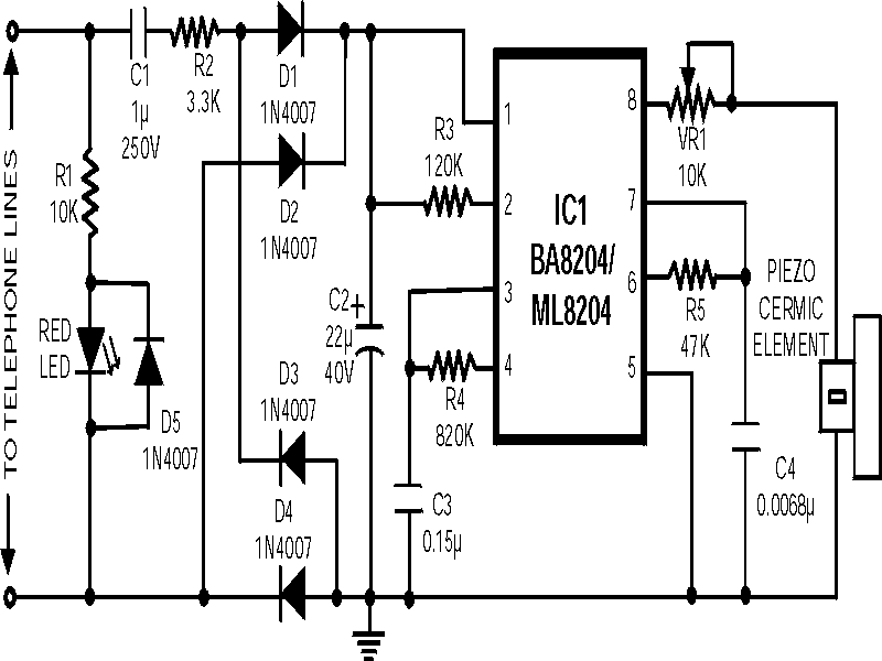
 Many a times one needs an ex- tra telephone ringer in an ad- joining room to know if there is an incoming call. For example, if the telephone is installed in the drawing room you may need an extra ringer in the bedroom. All that needs to be done is to connect the given circuit in parallel with the existing telephone lines using twin flexible wires. This circuit does not require any external power source for its operation. The section comprising resistor R1 and diodes D5 and LED1 provides a visual indication of the ring. Remaining part of the circuit is the audio ringer based on IC1 (BA8204 or ML8204). This integrated circuit, specially designed for telec- om application as bell sound generator, requires very few external parts. It is readily available in 8-pin mini DIP pack.

Resistor R3 is used for bell sensitivity adjustment. The bell frequency is controlled by resistor R5 and capacitor C4, and the repeat frequency is controlled by resistor R4 and capacitor C3. A little experimentation with the various values of the resistors and capacitors may be carried out to obtain desired pleasing tone. Working of the circuit is quite simple. The bell signal, approximately 75V AC, passes through capacitor C1 and resistor R2 and appears across the diode bridge comprising diodes D1 to D4. The rectified DC output is smoothed by capacitor C2. The dual-tone ring signal is output from pin 8 of IC1 and its volume is adjusted by volume control VR1. Thereafter, it is impressed on the piezo-ceramic sound generator

Off line Telephone tester


H ere is a circuit of an off-line telephone tester which does not require any telephone line for testing a telephone instrument. The circuit is so simple that it can be easily assembled even by a novice having very little knowledge of electronics. A telephone line may be considered to be a source of some 50 volts DC with a source impedance of about 1 kilo-ohm. During ringing, in place of DC, an AC voltage of 70 to 80 volts (at 17 to 25 Hz) is present across the telephone line. When the subscriber lifts the handset, the same is sensed by the telephone exchange and the ringing AC voltage is disconnected and DC is reconnected to the line. Lifting of the handset from the telephone cradle results in shunting of the lines two wires by low impedance of the telephone instrument. As a result, 50V DC level drops to about 12 volts across the telephone instrument. During conversation, the audio gets superimposed on this DC voltage. Since any DC supply can be used for testing a telephone instrument, the same is derived here from AC mains using step-down transformer X1. Middle point of the transformers secondary has been used as common for the two full-wave rectifiersone comprising diodes D1 and D2 together with smoothing capacitor C1 and the other formed by diodes D3 and D4 along with filter capacitor C2. The former supplies about 12 volts for the telephone instrument through primary of transformer X2 which thus simulates a source impedance, and a choke which blocks AC audio signals present in the secondary of transformer X2. The AF signal available in secondary of X2 is sufficiently strong to directly drive a 32-ohm headset which is connected to the circuit through headphone socket SK1 via rotary switch S2. During ringing, a pulsating DC voltage from transformer X1 via rectifier diode D5, push-to-on switch S3, and contact B of rotary switch S2 is applied across secondary of transformer X2. The boosted voltage available across primary of transformer X2 is sufficient to drive the ringer in the telephone instrument. Please avoid pressing of switch S3 for more than a few seconds at a time to prevent damage to the circuit due to high voltage across primary of transformer X2. The circuit also incorporates a music IC (UM66) whose output is connected to secondary of transformer X2 via switch S2 after suitably boosting its output with the help of darlington transistor pair T1 and T2. This output can be used to test the audio section of any telephone instrument. After having assembled the circuit satisfactorily, the following procedure may be followed for testing a telephone instrument:

1. Connect the telephone to the terminals marked To Telephone Under Testand switch on mains (switch S1).
2. To test the ringer portion, flip switch S2 to position B and press S3 for a moment. You should hear the ring in case the ringer circuit of the telephone under test is working. Please ensure that handset is on cradle during this test.
3. For testing the audio section, flip switch S1 to position C and connect a headphone to socket SK1. Pick the telephone handset and speak into its microphone. If audio section is working satisfactorily, you should be able to hear your speach via the headphone. If you dial a number, you should be able to hear the pulse clicks or pulse tone in the headphone, depending on whether the telephone under test is functioning in pulse or tone mode. If the telephone under test has a built-in musical hold facility, on pressing the hold button you should be able to hear the music. Now flip switch S2 to position A. You should be able to hear music generated by IC1 through earpiece of the handset of the telephone under test, indicating propor functioning of the AF amplifier section. The circuit can be assembled on a small piece of veroboard. Try to mount the two transformers on opposite sides of the board, displaced by 90 degrees. Always keep handy multi-type modular plugs for testing various types of telephones. Mount all switches, sockets and LEDs on the front of testing panel

The Link Telephone Intercom


The Link circuitry is simple and efficient, employing just two ICs, half a dozen transistors, and a handful of garden variety components. It all runs on 12 volts and is easily assembled. You can have your own home intercom between the kitchen, the garage, the rumpus room and at your poolside 'barby' and all for less than $100!
The Link intercom has been designed in such a way that you can buy parts for it off the shelf at just about any decent electronics retail chain. It uses old pulse dial handsets and replaces the AC bell set with a 9 volt DC buzzer. The whole circuit runs from a 12 volt regulated DC supply and is suitable for short term battery operation (eg: Gel Cell). It is suitable for radio field days and sporting events (providing you can scrounge enough 4 wire cable) and may find a place in pre-schools, old folks homes, boy scout/girl guide halls, churches, kids tree houses/fortresses, or maybe even more serious uses such as small offices, factories, workshops and many other applications.

The Link is designed to enable one call at a time within a small area (about 100 meters from the black box is about the max per handset) and is not suitable for connection to the PSTN (public network) as the voltages and currents used by the PSTN are higher, and will damage the simpler 12 volt circuitry, that employs CMOS ICs etc. The Link will run quite happily off a 12 volt regulated DC supply of only 200mA or so, and this can be a simple affair, such as a DC plug pack, wired to a 7812 regulator chip and appropriate filter caps on the output. Add some leds if you want!

Overview
The Link telephone intercom is designed around two ICs. The first, IC1, is an NE 556 dual timer chip, which is wired up to provide dial tone, ring tone (busy tone too, which will be explained along with a few add-ons to be mentioned later on) and ring pulses for the ringer circuit attached to each line circuit. The other chip, IC 2, is a CD 4017B decade counter, which is wired to count each train of dial pulses as they are received and buffered by the two opto-couplers, OC1 and OC 2 and their associated R/C networks.

Line Circuits
Each phone handset is connected by a four wire circuit from the black box Two wires (normally tagged 'white' and 'blue' here in Oz) are for speech and dialing functions, whereas the other two (tagged locally as 'red' and 'black') are for the ring pulses supplied by the ringer circuit to each DC buzzer inside the handsets. When a phone (eg: #1 for our discussion) is picked up in its 'off hook' condition, a DC loop is formed by the following components: DC circuitry inside the phone, the 1K winding of transformer TX, and back to 0V- earth. Taken from the +12 volts terminal, through the Leds inside OC1 and OC2 and back to the phone handset. 

Making A Call
Dial tone is provided to the calling partys phone when the Link is in its 'reset' condition (no calls in progress) via capacitor C3 and the 8 ohm winding (8R) of TX to 0v- earth. This and the other service tones are generated by IC1a, while ring pulses are generated by IC1b. When a calling party's phone is off hook, the leds 'force the photo transistors to switch on hard, pulling pins 13 and 14 of IC2 to 0 volts ground. When the dial inside the phone handset is pulled back and released, the collector lead of OC2's transistor is held low at 0 volts by the slow release charging of C5. Pin 13 of IC2 is a CE (chip enable) input, and needs to stay at a logic low (near 0 volts) to enable pin 14 to count the dial pulses. So while 'impulsing' occurs, pin 13 stays low, and pin 14 alternates between logic high and low as the led emulates each dial pulse train, until the last pulse in the train is received.

Dialing Into The Register
When caller number #1 dials phone number  # 4, those four pulses appear across the leds inside OC1 and OC2. The decade counter, acting as a Register (a storage device used in communications equipment for storing dialed digits) counts these pulses, turning its output pins on and off inn unison, with the last dial pulse causing the counter to rest on the last output pin that is turned on. The complete sequence for a maximum of ten pulses in the one pulse train, is (pin 3 is always at logic high at 'reset') 2,4,7,10, and then 1,5,6,9,11 and then finally pin 3. So when the number '4' is dialed, the counter would step through pins 2,4,7, and then land on pin 10, which is connected to phone #4's ringer circuit via Q4's base lead.

The Ringer Circuit
Each line circuit consists of the individual phone handset, the DC buzzer mounted inside it, the common connections to TX and the cathode of OC2s led, as well as transistors Q1 to Q4 and common driver transistor Q5. With pin 3 of IC2 at logic high on 'reset', diode D3 enables IC2a to provide a Dial Tone from pin 5. When a number is dialed, pin 3 of IC2 goes low on the first dial pulse, removing the logic high via D4 from pins 12 and 8 of IC1b, thus enabling it to charge up C3, and produce ring pulses to IC1a via diode D5, (from pin 9 to pin 4). After about 2 seconds, ring pulses commence, and the modulated dial tone (which then by default becomes an interrupted Ring Tone to the caller) is produced at pin 5 of IC1a, indicating the progress of the call.

True Ring Trip
When the called party answers the call, transistor QX with trimpot R6, (adjusted to detect both phones being 'off-hook',) triggers the led and phototransistor inside OC3. This halts the ring pulses and ring tone supplied by IC1a and IC1b for the duration of that call, by supplying a logic high potential to pins 12 and 8 of IC1b via D6. When the call is over, and both parties have hung up their phone handsets (eg: back to the on-hook status,) the DC loop formed by the handsets, TX and OC1/OC2 is broken. Pin 13 of IC2 returns to its reset potential of logic high, and extends this high to pin 15 (Reset) of the 4017 decade counter chip, which disables the output selected during the dialing operation, and enables pin 3 to high, thus restoring Dial Tone to the next caller via pin 4 of IC1a.

Resetting The Link
 Thus the Link is fully reset and ready for another call. As you can see, it may seem a little complicated to follow the progression through a call, particularly if you havent been involved with phones and logic chips much before. At the end of the day, you have some simple counting, pulsing and interfacing circuitry, which will perform all the necessary tasks of a basic intercom, and all at a reasonable cost. I used some formatted matrix board for the p.c.b and IC sockets for all ICs and OC/OC2. I also found that a heat sink fin for the 7812 regulator chip was unnecessary. A box could be used for housing the Link circuitry, and some kind of screw terminal block or ID block (like a small 10 pair KRONE junction box) could be used to terminate the wiring at the box to make it look more professional. Remember these two things. If you leave a phone off-hook you will lock up the Link and if you pick up a phone when someone else is dialing, wrong numbers will result. Apart from that, have fun!

Parts List:
R10             100k
R1              10k
R2              150k
R3              4k7
R4              47k
R5              2k2
R6              4k7 trimpot
R7              390R
R8              10k
R9              100k
R11             22k
R12-R15    2k2
R16             4k7
R17             4k7
C1              0.22uF
C2              47uF
C3              1uF
C4              2,200uF (power filter cap  not shown, but wired across +12volts & 0v- ground points
Q1-Q5           BC547 n.p.n low gain
Q6              BC 549C high gain with a beta of at least 250+

D1-D7           1N4148 or 1N914 small signal diodes
IC1             NE 556 dual timer chip
IC2             CD 4017B decade counter chip
OC1-OC3 4N25 or 4N28 opto couplers
Tx              1k/8R transformer, with 1k centre tapped
B1-B4           9 volt DC buzzers mounted inside phone handsets

Audio Visual Indicator for Telephones


Many a times one needs an extra telephone ringer in an ad joining room to know if there is an incoming call. For example, if the telephone is installed in the drawing room you may need an extra ringer in the bedroom. All that needs to be done is to connect the given circuit in parallel with the existing telephone lines using twin flexible wires. This circuit does not require any external power source for its operation. The section comprising resistor R1 and diodes D5 and LED1 provides a visual indication of the ring. Remaining part of the circuit is the audio ringer based on IC1 (BA8204 or ML8204). This integrated circuit, specially designed for telecom application as bell sound generator, requires very few external parts. It is readily available in 8-pin mini DIP pack.

Resistor R3 is used for bell sensitivity adjustment. The bell frequency is controlled by resistor R5 and capacitor C4, and the repeat frequency is controlled by resistor R4 and capacitor C3. A little experimentation with the various values of the resistors and capacitors may be carried out to obtain desired pleasing tone. Working of the circuit is quite simple. The bell signal, approximately 75V AC, passes through capacitor C1 and resistor R2 and appears across the diode bridge comprising diodes D1 to D4. The rectified DC output is smoothed by capacitor C2. The dual-tone ring signal is output from pin 8 of IC1 and its volume is adjusted by volume control VR1. Thereafter, it is impressed on the piezo-ceramic sound generator.

Off Line Telephone Tester Circuit Diagram


Here is a circuit of an off-line telephone tester which does not require any telephone line for testing a telephone instrument. The circuit is so simple that it can be easily assembled even by a novice having very little knowledge of electronics. A telephone line may be considered to be a source of some 50 volts DC with a source impedance of about 1 kilo-ohm. During ringing, in place of DC, an AC voltage of 70 to 80 volts (at 17 to 25 Hz) is present across the telephone line. When the subscriber lifts the handset, the same is sensed by the telephone exchange and the ringing AC voltage is disconnected and DC is reconnected to the line. Lifting of the handset from the telephone cradle results in shunting of the line’s two wires by low impedance of the telephone instrument. As a result, 50V DC level drops to about 12 volts across the telephone instrument. During conversation, the audio gets superimposed on this DC voltage. Since any DC supply can be used for testing a telephone instrument, the same is derived here from AC mains using step-down transformer X1. Middle point of the transformer’s secondary has been used as common for the two full-wave rectifiers—one comprising diodes D1 and D2 together with smoothing capacitor C1 and the other formed by diodes D3 and D4 along with filter capacitor C2. The former supplies about 12 volts for the telephone instrument through primary of transformer X2 which thus simulates a source impedance, and a choke which blocks AC audio signals present in the secondary of transformer X2. The AF signal available in secondary of X2 is sufficiently strong to directly drive a 32-ohm headset which is connected to the circuit through headphone socket SK1 via rotary switch S2. During ringing, a pulsating DC voltage from transformer X1 via rectifier diode D5, push-to-on switch S3, and contact ‘B’ of rotary switch S2 is applied across secondary of transformer X2. The boosted voltage available across primary of transformer X2 is sufficient to drive the ringer in the telephone instrument. Please avoid pressing of switch S3 for more than a few seconds at a time to prevent damage to the circuit due to high voltage across primary of transformer X2. The circuit also incorporates a music IC (UM66) whose output is connected to secondary of transformer X2 via switch S2 after suitably boosting its output with the help of darlington transistor pair T1 and T2. This output can be used to test the audio section of any telephone instrument. After having assembled the circuit satisfactorily, the following procedure may be followed for testing a telephone instrument:
1. Connect the telephone to the terminals marked ‘To Telephone Under Test’and switch on mains (switch S1).
2. To test the ringer portion, flip switch S2 to position ‘B’ and press S3 for a moment. You should hear the ring in case the ringer circuit of the telephone under test is working. Please ensure that handset is on cradle during this test.
3. For testing the audio section, flip switch S1 to position ‘C’ and connect a headphone to socket SK1. Pick the telephone handset and speak into its microphone. If audio section is working satisfactorily, you should be able to hear your speach via the headphone. If you dial a number, you should be able to hear the pulse clicks or pulse tone in the headphone, depending on whether the telephone under test is functioning in pulse or tone mode. If the telephone under test has a built-in musical hold facility, on pressing the ‘hold’ button you should be able to hear the music. Now flip switch S2 to position ‘A’. You should be able to hear music generated by IC1 through earpiece of the handset of the telephone under test, indicating propor functioning of the AF amplifier section. The circuit can be assembled on a small piece of veroboard. Try to mount the two transformers on opposite sides of the board, displaced by 90 degrees. Always keep handy multi-type modular plugs for testing various types of telephones. Mount all switches, sockets and LEDs on the front of testing panel

Audio Visual Ringer Circuit Diagram


Many a times one needs an ex- tra telephone ringer in an ad- joining room to know if there is an incoming call. For example, if the telephone is installed in the drawing room you may need an extra ringer in the bedroom. All that needs to be done is to connect the given circuit in parallel with the existing telephone lines using twin flexible wires. This circuit does not require any external power source for its operation. The section comprising resistor R1 and diodes D5 and LED1 provides a visual indication of the ring. Remaining part of the circuit is the audio ringer based on IC1 (BA8204 or ML8204). This integrated circuit, specially designed for telec- om application as bell sound generator, requires very few external parts. It is readily available in 8-pin mini DIP pack.
Resistor R3 is used for bell sensitivity adjustment. The bell frequency is controlled by resistor R5 and capacitor C4, and the repeat frequency is controlled by resistor R4 and capacitor C3. A little experimentation with the various values of the resistors and capacitors may be carried out to obtain desired pleasing tone. Working of the circuit is quite simple. The bell signal, approximately 75V AC, passes through capacitor C1 and resistor R2 and appears across the diode bridge comprising diodes D1 to D4. The rectified DC output is smoothed by capacitor C2. The dual-tone ring signal is output from pin 8 of IC1 and its volume is adjusted by volume control VR1. Thereafter, it is impressed on the piezo-ceramic sound generator

Telephone Headgear Circuit Diagram


Acompact, inexpensive and low component count telecom head- set can be constructed using two readily available transistors and a few other electronic components. This circuit is very useful for hands-free operation of EPABX and pager communication. Since the circuit draws very little current, it is ideal for parallel operation with electronic telephone set. Working of the circuit is simple and straightforward. Resistor R1 and an ordinary neon glow- lamp forms a complete visual ringer circuit. This simple arrangement does not require a DC blocking capacitor because, under idle conditions, the telephone line voltage is insufficient to ionise the neon gas and thus the lamp does not light. Only when the ring signal is being received, it flashes at the ringing rate to indicate an incoming call. The bridge rectifier using diodes D1 through D4 acts as a polarity guard which protects the electronic circuit from any changes in the telephone line polarity. Zener diode D5 at the output of this bridge rectifier is used for additional circuit protection. Section comprising transistor T1, resistors R2, R3 and zener diode D6 forms a constant voltage regulator that provides a low voltage output of about 5 volts. Dial tone and speech signals from exchange are coupled to the receiving sound amplifier stage built around transistors T2 and related parts, i.e. resistors R7, R6 and capacitor C5. Amplified signals from collector of transistor T2 are connected to dynamic receiver RT-200 (used as earpiece) via capacitor C7. A condenser microphone, connected as shown in the circuit, is used as transmitter. Audio signals developed across the microphone are coupled to the base of transistor T1 via capacitor C3. Resistor R4 determines the DC bias required for the microphone. After amplification by transistor T1, the audio signals are coupled to the telephone lines via the diode bridge. The whole circuit can be wired on a very small PCB and housed in a medium size headphone, as shown in the illustration. For better results at low line currents, value of resistor R2 may be reduced after testing

Smart Phone Light Circuit Diagram


The circuit shown here is used to switch on a lamp when the tele- phone rings, if the ambient light is insufficient. The circuit uses only two ICs and it can be implemented very easily. A light dependent resistance (LDR), with about 5 kilo-ohms resistance in the ambient light and greather than 100 kilo-ohms in darkness, is at the heart of the circuit. The circuit is fully isolated from the phone lines and it draws current only when the phone rings. The circuit provides automatic switching on of a lamp during darkness when the phone is kept in a place such as the bedroom. The lamp can be battery powered to provide light during power failure or load shedding. This avoids delay in attending to a call. The light switches off automatically after a programmable time period and it needs no attention at all. If required, the lamp lighting period can be extended by simply pressing a pushbutton switch (S1). The first part of the circuit functions as a ring detector. When telephone is on-hook, around 48V DC is present across the TIP and RING terminals. The diode in the opto-coupler is ‘off’ during this condition and it draws practically no current from he telephone lines. The opto-coupler also isolates the circuit from the telephone lines. Transistor in the opto-coupler is normally ‘off’ and a voltage of +5V is present at the ring indicator line. When telephone rings, an AC voltage of around 70-80V AC, which is present across the telephone lines, is used to turn on the diode inside the opto-coupler (IC2) which in turn switches on transistor inside the opto-coupler. The voltage at its collector passes through 0-volt level during ringing to trigger IC3 74LS123(A) monostable flip-flop. The other opto-coupler (IC1) is used to detect the ambient light condition. When there is sufficient light, LDR has a low resistance of about 5 kilo-ohms and the transistor inside the opto-coupler is in ‘on’ state. When there is insufficient light available, the resistance of LDR increases to a few mega-ohms and the transistor switches to ‘off’ state. Thus the DC voltage present at the collector of transistor inside the opto-coupler is normally 0V and it jumps to 5V when there is no light or insufficient light. The 74LS123 retriggerable monostable multivibrator is used to generate a programmable pulse-width. The first monostable 74LS123(A) generates a pulse from the trigger input available during ringing, provided its pin 2 input (marked B) is logic high (i.e. during darkness). It remains high for the programmed duration and switches back to 0V at the end of the pulse period. This high-to-low transition (trailing edge) is used to trigger the second monostable flip-flop 74LS123(B) in the same package. Output of the second monostable is used to control a relay. The lamp being controlled via the N/O contacts of the relay gets switched ‘on.’ The ‘on’ period can be extended by simply pressing pushbutton switch S1. If nobody attends the phone, the light turns off automatically after the specific time period equal to the pulse-width of the second flip-flop. The light sensitivity of LDR can be changed by changing resistance R2 connected at collector of the transistor in light monitor circuit. Similarly, switch-on period of the lamp can be controlled by changing capacitor C3’s value in the second 74123(B) monostable circuit

Telephone Number Display Circuit Diagram


The given circuit, when connected in parallel to a telephone, dis- plays the number dialled from the telephone set using the DTMF mode. This circuit can also show the number dialled from the phone of the called party. This is particularly helpful for receiving any number over the phone lines. The DTMF signal—generated by the phone on dialling a number—is decoded by DTMF decoder CM8870P1 (IC1), which converts the received DTMF signal into its equivalent BCD number that corresponds to the dialled number. This binary number is stored sequentially in 10 latches each time a number is dialled from the phone. The first number is stored in IC5A (1/2 of CD4508) while the second number is stored in IC5B and so on. The binary output from IC1 for digit ‘0’ as decoded by IC1 is 10102 (=1010), and this cannot be displayed by the seven-segment decoder, IC10. Therefore the binary output of IC1 is passed through a logic-circuit which converts an input of ‘10102’ into ‘00002’ without affecting the inputs ‘1’ through ‘9’. This is accomplished by gates N13 through N15 (IC11) and N1 (IC12). The storing of numbers in respective latches is done by IC2 (4017). The data valid output from pin 15 of IC1 is used to clock IC2. The ten outputs of IC2 are sequentially connected to the store and clear inputs of all the latches, except the last one, where the clear input is tied to ground. When an output pin of IC2 is high, the corresponding latch is cleared of previous data and kept ready for storing new data. Then, on clocking IC2, the same pin becomes low and the data present at the inputs of that latch at that instant gets stored and the next latch is cleared and kept ready. The similar input and output pins of all latches are connected together to form two separate input and output buses. There is only one 7-segment decoder/driver IC10 for all the ten displays. This not only reduces size and cost but reduces power requirement too. The output from a latch is available only when its disable pins (3 and 15) are brought low. This is done by IC3, IC12 and IC13. IC3 is clocked by an astable multivibrator IC4 (555). IC3 also drives the displays by switching corresponding transistors. When a latch is enabled, its corresponding display is turned on and the content of that latch, after decoding by IC10, gets displayed in the corresponding display. For instance, contents of IC5A are displayed on display ‘DIS1,’ that of IC5B on ‘DIS2’ and so on. The system should be connected to the telephone lines via a DPDT switch (not shown) for manual switching, otherwise any circuit capable of sensing handset’s off-hook condition and thereby switching relays, etc. can be used for automatic switching. The power-supply switch can also be replaced then. Though this circuit is capable of showing a maximum of ten digits, one can reduce the display digits as required. For doing this, connect the reset pin of IC2, say, for a 7-digit display, with S6 output at pin 5. The present circuit can be built on a veroboard and housed in a suitable box. The displays are common-cathode type. To make the system compact, small, 7-segment displays can be used but with some extra cost. Also, different colour displays can be used for the first three or four digits to separate the exchange code/STD code, etc. The circuit can be suitably adopted for calling-line display

Cordless Phone Backup


Normally the base of a cordless phone has an adaptor and the handset has Ni-Cd cells for its operation. The base unit becomes inoperative in case of power failure. In such conditions, it is better to provide a backup using Ni-Cd cells externally. Here is a simple circuit which can be used with cordless phone SANYO CLT-420 or similar sets.
The working is simple. When AC mains is present, Ni-Cd cells are charged through IC LM317L, which is wired as a current source. Also, diode D3 is reverse-biased, which keeps Ni-Cd cells isolated from positive rail. When AC mains goes off, the Ni-Cd cells provide supply to the cordless phone base unit through diode D3. A green LED is used to indicate the presence of AC mains.
Each Ni-Cd cell costs around Rs 34, and the cost of the backup unit, including the box and cells, would not exceed Rs 300. Hence the circuit is well worth the investment

Multipurpose Circuit For Telephone


This add-on device for telephones can be connected in parallel to the telephone instrument.
The circuit provides audio-visual indication of on-hook, off-hook, and ringing modes. It can also be used to connect the telephone to a cid (caller identification device) through a relay and also to indicate tapping or misuse of telephone lines by sounding a buzzer.

In on-hook mode, 48V dc supply is maintained across the telephone lines. In this case, the bi-colour led glows in green, indicating the idle state of the telephone. The value of resistor r1 can be changed somewhat to adjust the led glow, without loading the telephone lines (by trial and error).

In on-hook mode of the hand-set, potentiometer vr1 is so adjusted that base of t1 (bc547) is forward biased, which, in turn, cuts off transistor t2 (bc108). While adjusting potmeter vr1, ensure that the led glows only in green and not in red.

When the hand-set is lifted, the voltage drops to around 12V dc. When this happens, the voltage across transistor t1’s base-emitter junction falls below its conduction level to cut it off. As a result transistor pair t2-t3 starts oscillating and the piezo-buzzer starts beeping (with switch s1 in on position). At the same time, the bi-colour led glows in red.

In ringing mode, the bi-colour led flashes in green in synchronisation with the telephone ring.

A cid can be connected using a relay. The relay driver transistor can be connected via point a as shown in the circuit. To use the circuit for warning against misuse, switch s1 can be left in on position to activate the piezo-buzzer when anyone tries to tap the telephone line. (When the telephone line is tapped, it’s like the off-hook mode of the telephone hand-set.)

Two 1.5V pencil cells can provide Vcc1 power supply, while a separate power supply for Vcc2 is recommended to avoid draining the battery. However, a single 6-volt supply source can be used in conjunction with a 3.3V zener diode to cater to both Vcc2 and Vcc1 supplies

 
Design by Free WordPress Themes | Bloggerized by Lasantha - Premium Blogger Themes | cheap international calls