Low Power Under- and Over-Voltage Monitor

This voltage monitor has two  threshold, VTH for undervoltage and VTH’ for overvoltage. Using the component values shown in the schematic diagram below, this circuit give 6V for VTH and 15V for VTH1. Above 6V, the LED indicator of this voltage monitor  circuit will increase the flash rate until reach 15V.  This circuit will stop flashing at voltage below 6V and above 15 volts since there will be no current flowing through C1.  At threshold  boundary, the output of LM10 will saturate to negative below VTH and saturate to positive above VTH’.

To customize circuit we can select the resistors values according to chosen VTH and VTH’ using the following formula:
VTH=[R4(R1+R2)Vref]/[R1(R3+R4)];
VTH’=[R4(R1+R2)Vref]/[R1(R3+R4)-R3(R1+R2)]
Since the current consumption is very small (around 500uA), this voltage monitor will be suitable for various application  demanding low cost solution,  such as battery monitoring, small testing equipments, or power line indication.

5V FET Voltage Regulator

This voltage regulator circuit gives a stable 5V output from unregulated inputs (more than 5V). The stability of the output voltage is good enough, only change less than 0.1 volts when the load current changes about 60mA. Here is the schematic diagram of the circuit:

 The basic principle of the voltage regulation rely on the mechanism of keeping the the FET’s gate voltage at the cut-off point. The FET’s gate volage is the voltage across R2. At zero volt (when there is no current flowing through R2), the FET will be conducting, and a small current at FET (Tr1) will cause much larger current to flow through Tr3. This current will flow  through R2 and the gate voltage becomes negative. A some level the negative voltage at FET’s gate will cut-off the FETs current and  keep the output voltage stable

26V-to-5000V DC-DC Converter

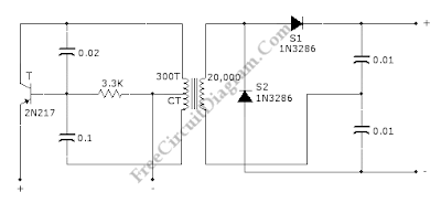
This circuit can provide 5,000 VDC from 26 VDC. This circuit has ripple of under 0.01% due to Voltage-doubling capacitors. As sinusoidal oscillator, a 2N217 transistor is used. The diode and the capacitors at the output stage should be of high voltage type.  Here is the schematic diagram of the  circuit:

Transceiver Saver (Overvoltage Protector)

This is a transceiver saver circuit that protect  a transceiver device (applicable to other device as well)  from overvoltage of the power supply. This circuit is used to protect the device  by regulating the power supply,  avoiding damaging the device if overvoltage occurs.  If the transceiver transmits current of above 2A, a heatsink should be used for the transistor. The value of resistor must provide output of 12.6 V during normal operation, you can make trial and error through measurement when choosing this., you can start with value around 100R. It’s recommended to use a high wattage Zener diode. Here is the schematic diagram of the circuit:

Auto-Off 12V NiCd Battery Charger

NiCd/NiCad battery charger circuit is still needed since some application demanding high current is still rely on NiCd type, since this type is still superior in term of  high current output (low internal resistance) and low cost. This  battery charger circuit is used to charge 12V NiCd battery at  around 74 mA until battery is fully  charged. This circuit need  around 4 hours to fully recharge a totally empty/dead battery, depends on the battery capacity.  Here is the schematic diagram of the circuit


 This circuit is basically a current source with auto cut-off. The current regulation is done by maintaining a fix voltage across a 68R at the emitter of  2N2219 transistor. This voltage is stabilized by a 5.6V zener diode 1N752, which keep the voltage at 68R resistor at around 5V, giving a constant current of 74 mA.  The auto-off feature work by monitoring the output voltage (before the 1N4001 diode) relative to ground, as this voltage increases in accordance with the battery voltage which is being charged.  After the battery voltage reach the fully-charged level, the lower 1N752 zener diode will pass the current to activate the 2N222 transistor, which short the upper transistor’s base, turning off the charging process. To calibrate the shut off point, connect a 270 ohm / 2 Watt  resistor across the charge terminal and adjust the pot until the charging terminal voltage  show 15.5V level

Foldback Current Limited High Voltage Regulator

This circuit is high voltage regulator which has foldback current limiter protection. This circuit uses LM10 comparator with voltage reference, and this core integrated circuit is connected directly to high voltage circuitry. This high voltage direct connection is possible since the IC is inserted to a bias network and directly drop the applied voltage, so this IC is only suffering small voltage across its supply pins.

 The foldback current limiter is different with ordinary current limiter in the way the limiter responds to dynamic load. When we plot the regular current limiter, when the load draw a linearly increasing current, the plot of the current will be linear ramp which stops at a specified level determined by the limiter. A foldback current limiter will give same response until the current reach the maximum level, but will fold the current back to a much lower current level if the load try to further increase the current. This foldback action will prevent the final driver  transistor in the regulator from overheating

1 KW Power (Watt) Meter

This watt-meter circuit has measurement range up to 1-KW. This circuit can give the complete (X)(Y) function although uses only one transistor. Actually, this circuit is used for 117 Vac±50 Vac operation. For lower or lower voltage, this circuit can be modified easily. This circuit only measure power on negative cycles. The advantages of this circuit is this circuit does not need external power supply. This circuit measures true power that is delivered to the load. Here is the schematic diagram of the  circuit:


 At idle section, this circuit draw only 0.5W. This circuit has load current-sensing voltage of 10mV and load voltage loss of 0.01%. For linear loads, Rejection of reactive load currents is better than 100:1. When using a 50-μA meter movement, the nonlinearity of this circuit is about 1% full scale. Copper shunt can be used to give correct gain due to temperature

Simple Theremin with Inverter Gates

This simple but complete Theremin circuit is constructed using only two inverter chip plus one regulator IC. This Theremin circuit consist of five functional blocks: power supply regulator, hand controlled oscillator, null oscillator, mixer, and filter

The power supply regulator consist of LP2950 regulator IC, which stabilize the voltage from battery to 5V. You can use more popular 7805 IC for this, but since the power consumption of this Theremin circuit is very small, then you can use 78L05 which is smaller.  CR1 diode is used to protect from inappropriate battery polarity,  shorting the battery voltage together with R8 100 Ohm resistor which prevent the large current when the battery is installed in wrong direction. Although the inverter chip will work well for 9V battery, there is a benefit of using voltage regulation to regulate the battery voltage at lower voltage level, that the voltage will remain constant for until the end of battery life. This will avoid frequency drift of the Theremin’s null oscillator  which should be carefully adjusted to zero the output frequency, which can be affected by the supply  voltage.
Hand Controlled Oscillator
The hand proximity sensor is an oscillator which has antenna extension which shift the capacity coupling in the loop. This capacitance shift occur when we move our hand approaching the antenna. Since this change is very small in percentage, we need this oscillator to be high enough to produce notable frequency difference.  This oscillator block is built around U1A, U1B, and U1C. This oscillator give oscillation at around 73kHz. This frequency is not directly audible, we have to process this signal further to produce audible signal.
Null Oscillator
Null oscillator is employed to produce a constant frequency oscillation that will be used to produce differential frequency which is audible.  This oscillator block is built around U2A, U2B, and U2C. This null oscillator should be adjustable to set the null point where the Theremin should produce no oscillation at certain hand position.  At this point, the null oscillator should be adjusted to have  same frequency with the hand controlled oscillator since the audible Theremin output is the product of the difference between hand controlled and null oscillator frequencies.
Frequency Mixer (Differentiator)
The mixer is used to mix the signal from two oscillators, the hand controlled and the null oscillators. This mixer produce an output which contain many frequency components, not only the difference but also the original and the sum, since the amplifier U1F is basically a digital inverter which has non-linear transfer function. Fortunately, all the frequency components, except the difference, will be much higher than the needed signal and inaudible. This make it easy to remove by simple low pass filter to obtain only the differential frequency component.
Low Pass Filter
As stated before, we need to obtain only the audible frequency component by low-pass filtering. Although the high frequencies is inaudible, we still have to remove it since it can cause damage in audio power amplifier is the level is too high. It can distort the audible signal, and it can eat the electric power like ghost, frying your amplifier or at least make it overheated. This  Theremin circuit use simple low pass filter consist of C4, R5, and R7 for the passive stage, and C2 inside the inverter amp loop.

True Stereo Indicator Detects L-R Signal Difference

This true stereo indicator is different from what we usually find on FM radio receiver, which is usually a pilot tone detector. A stereo broadcast from FM radio station contain pilot tone, but a presence of pilot tone doesn’t necessarily a stereo broadcast signal since a mono FM transmitter ca broadcast pilot tone as well.  Since this circuit detect the difference between left and right channel, this circuit can detect a real stereophonic programs. When there is no difference between R and L input signals, the output A1 and output A2 is at the same potential. That will make a a virtual ground rail at half the supply voltage.

The A1 will supply a negative or positive voltage when A1 detects a difference between R and L input signals with respect to the virtual ground rail. The C4 will be charged via D2 an C3 via D1. The LED is turned on by the comparator A3/A4 via OR circuit D3/D4. The input signal level should be greater than 100mV to compensate for the drop across D2 or D1. P1 is used to adjust the sensitivity of stereo indicator.

53 dB Stereo Preamp for Tape or Phonographs

With the circuit shown in the following schematic diagram, both channels of this stereo preamp is constructed using  RCA CA3052 quad AC amplifier.  this pre-amplifier circuit is featured with tone control (bass – treble). Make a similar circuit to complete the other channel, since the circuit for left and right channel are similar. To be high-fidelity, total harmonic distortion should be kept minimum, this circuit gives less than 0.3% distortion level at  at 1-kHz testing signal with 1-V amplitude.  Gain or amplification at 1 kHz is 47 dB,  and the tone control will curve the response with 11.5-dB boost at 100 Hz and 10 kHz at maximum bass and treble boost.  For minimum bass and treble knob position,  the attenuation will be 10dB  at 100 Hz  and 9dB at 10kHz. This circuit is operated by a single ended supply for wider range environment. Inputs can be from tape recorders pickup or magnetic-cartridge phonographs.

Simple 9V Wireless Microphone FM Transmitter

This FM transmitter circuit can be used as a wireless microphone,  can be received by an ordinary 88- to 108-MHz FM broadcast receiver. For the power supply, this transmitter circuit is powered by a 9 V battery. To comply with the radiation limit of FCC rules, keep the antenna length under 12 inches. L1 is 6 turns of #24 wire wound around a pencil or a 1/4″ form, with turns spacing of 1 wire diameter. C6 is a gimmick capacitor which has value about 1 pF.

LM380, Simple 2 Watts Audio Amplifier

Small audio amplifier is useful for audio troubleshooting or simple audio projects. It should be a low cost and easy to build. Using integrated circuit for this purpose is the right choice. With LM380  audio amplifier integrated circuit, 2 Watts power can be delivered. For better thermal endurance, a large copper track can be printed in the board to provide heat sinking, this copper track should be soldered to pins 4, 3, 10, 5, 12 and 11.

Direct High Voltage DC Regulator

This regulator circuit stabilize the output voltage at 200V directly (without a transformer). Although the output voltage is high, this circuit only suffer a tension of the voltage drop (Vinput-Voutput), which is suffered mainly by the transistors. The op-amp suffers even less tension, since it regulate the applied voltage at their pins around the level of transistor’s bias voltage level.

Discrete Sliding Tone (Frequency Ramp) Doorbell

This doorbell circuit produces a low tone that will slide up to higher frequency. The equivalent total resistance connected between the base of Q1 and ground (Rbg) , and coupling capacitor  C1  determines the AF oscillator’s frequency. The resistance (Rbg) is equal to (R2+R1)R3. 

The R2 is used to set the initial bias condition, adjusted to produce a pleasant low starting frequency doorbell tone. D1 will start to conduct when Capacitor C3 charge through R6 until it reaches D1 bias  voltage level. Then the value of Rbg is paralleled by R4 and D1, and R5-D2-D3, and the values of diode’s equivalent resistance is gradually decreased as the C3 voltage ramp up.  This decreasing resistance value make the output tone slides up in frequency.  Two different diode path is provided to extend the linear area of diode conduction transition slope. With two path with different biases, after the single diode path has saturated, the second path provide further linear increase at higher voltage level.

LM3900 Audio Mixer

This audio mixer circuit doesn’t use a low impedance input to mix no ideal  sources, but use many amplifiers to provide  ideal sources before mixed through simple resistors. Ideal source means a sources with low impedances, make the interaction between signals in the output doesn’t affect the input.   Please note that this mixer circuit has high impedance output, so you’ll need an next processing equipment with appropriate  input specs. This audio mixer circuit is designed around an LM3900 quad op amp and combines 2 line and 2 mike inputs and sums them at the output terminal. To vary the gain (around +23 dB), we can change the R7 through R10.

Power Saver for Relays

Relays are normally operated at current level where it can initiate the mechanical metal contactors movement. After contacts has been established, the current level needed to keep the conductor plates stay attached is actually smaller than the current to initiate it. This power saver circuit seems to have opposite mechanism of surge protector. This circuit provide surge current to initiate mechanical movement, but after that, this circuit throttle the current to save the power, provide lower current level just to keep the contacts stay attached

The mechanism of this circuit is similar but done in opposite way with current surge protector. If we use a varistor with negative coefficient, here we use a kind of varistor but with positive coefficient, where the resistance increases as the temperature increase. This kind of varistor is actually an incandescent bulbs, two bulbs in parallel. At cold temperature, this bulbs has very low resistance, this make sure the relay will has sufficient power supply to initiate the mechanical movement of  its contactors. After the relay works, the rise of bulbs temperature will make the current decreased to a lower level, saving the power while maintaining the contactors stay attached. That’s all the mechanism of this power saver circuit.

TDA7056 3W BTL Mono Audio Power Amplifier


For mono output amplifier application,  TDA7056  IC can be your option. Compact but powerful, this integrated circuit is contained in a 9 pin medium power package. This device is designed for battery fed portable equipments such as mono recorders, radios and television. To attract the market, TDA7056 has many features such as low power consumption. For more reliable operation, TDA7056 also has short circuit proof and ESD (Electro Static Discharge) protected on all pins.  Designing application with this IC should be easy since no external components is needed. To make sure you’ll love this chip, this device also has no switch on/off clicks. Overall, TDA7056 has good stability.

Compressor Circuit with 570/571 Compandor IC


Compressor circuit provide high gain for low amplitude input and provide low gain for high amplitude input. This action, in effect, produce a nearly constant amplitude even though the input has very high dynamic range (very high amplitude variation from time to time). The action of compression like this is needed in some situation, such as in maximizing modulation depth in broadcasting, or sustaining electric guitar signal which has very high variation between the plucking time and fading out.  The following circuit has complementary input/output characteristic and unity gain at 0.775 VRMS input. Voltage gain through compressor is square root of 0.7/Vin. Vin is average input voltage. This circuit  uses Signetics dual channel compandor IC.  570 has lower inherent distortion and higher supply voltage range (6-24 V) than 571 (6-18 V).

Sound-Activated Lamp (Relay/Switch)


This simple circuit shown int the schematic diagram actives the switch using sound. We can use this circuit for various applications, such as automatic (sound-controlled) disco light or car’s LED light show.  The Q1 amplify the audio from mic. The R1 is used to adjust the peak of signal to greater than about 0.7 volts, act as sensitivity adjuster. A certain level, the signal coming from microphone, after amplification by Q1, will trigger the SCR and light lamp I1. If we change the lamp with a relay, then we can get a sound-activated relay/switch, which can be used to control more powerful / high wattage high voltage lamps. If we use a relay, place a 1N4007 diode in parallel with the relay coil to prevent the back-emf from  relay coil destroying the SCR.

Basic Complementary (Push-Pull) Power Amplifier Circuit


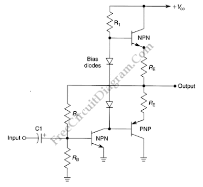
This amplifier circuit is very popular audio power amplifier circuit type. We call it a complementary since the final transistors is an NPN-PNP pair, each with the same characteristics. This circuit produce an AB class amplifier, since each transistor works in slightly more than half cycle of the signal. There is overlap area when both transistor conduct a current, and this area will be around its stationary current (when the input signal is zero). This circuit is also known as push-pull amplifier circuit since each transistor in the pair is working alternatively.

LM3900 Audio Mixer


This audio mixer circuit doesn’t use a low impedance input to mix no ideal  sources, but use many amplifiers to provide  ideal sources before mixed through simple resistors. Ideal source means a sources with low impedances, make the interaction between signals in the output doesn’t affect the input.   Please note that this mixer circuit has high impedance output, so you’ll need an next processing equipment with appropriate  input specs. This audio mixer circuit is designed around an LM3900 quad op amp and combines 2 line and 2 mike inputs and sums them at the output terminal. To vary the gain (around +23 dB), we can change the R7 through R10.

Ni-Cad Battery Zapper, A Rechargeable Battery Reconditioner


Ni-Cad (NiCd, NiCad) battery, sometimes doesn’t work as expected, gives no power and cannot be recharged. In this situation, the battery need to be reconditioned. It’ is possible that the battery is internally shorted, and we can get the battery into life again by recondition the Ni-Cad battery using a zapper circuit. This circuit restore the Ni-Cad battery from shorting by forcing a high current flow to burn the internal dirt. The current stored in the high capacitance capacitor is heavy discharged by the SCR when zapping, and the SCR is used to disconnect the battery connection when charging the capacitor. A 120 ohm 10W resistor is used to limit the current when charging the capacitor, and you have to make sure the LED’s intensity has reach the steady state before switching to zap position. After zapping the battery and switch to charge position, the charging process will take some period and indicated by the LED which will gradually increase the brightness until get stable intensity when fully charged. The power supply for this circuit can be taken from small transformer (350 mA to 1 A) with half or full wave rectifier. Here is the schematic diagram of the battery zapper circuit:

Main Power-Battery Backup Switcher


The schematic diagram shown below is a battery backup regulator circuit, useful for memory or other low power (battery operated) but critical circuit (must continue operation on powerline failure). The one LT020 will not conduct in under line-powered condition, made possible by means of of feedback string’s arrangement. In case of main power failure, the battery-driven LT1020 will turn on and maintain the load, when the line LT1020 go off because the line goes down.

High-Voltage Generator with HEX FET


The schematic diagram below show a circuit of high voltage generator. This circuit uses a 4049 hex inverter as an oscillator, and you can use ignition transformer from automotive engine. A fly-back transformer is possibly usable too. The 4049 will drive the IRF731 HEX FET. The Q1 must be heatsinked. Here is the schematic diagram of the circuit:

Voltage-Controlled Attenuator (Volume Control) Using FET


Using the circuit shown in the schematic diagram below, we can control the low-level audio signals with ±3V variable DC voltage. This attenuator circuit uses a field effect transistor (FET) to shunt the signal to ground. The R2 is used to control the output level (the attenuation level), but you can use other source of voltage signal to control the grid of the FET, such as DAC output, just remember that this voltage is a negative going signal (you can use with DAC which uses symmetric power supply system). The minimum output of this circuit is when gate bias is zero. When the gate bias is set close to pinchoff value, the circuit will produce maximum output with value that equal to input level. Here is the schematic diagram of the circuit:

60-dB Range Compressor For Audio


A compressor circuit shown in the schematic diagram below can produce consistent output of 1.4V P-P over entire 60dB range that is very useful for audio level/volume stabilization.  As the main components, this circuit uses a 741 opamp and JFET. With input range of 20mV to 2oV, this circuit has delay time of 0.4s (decay time)  and response time of 1.2ms (attack time). The JFET is used as  voltage-controlled resistor in peak-detecting control loop of 741 opamp.

Three Cells Produce Regulated 3V – 3.3V


Three NiCad and NiMH batteries can be used to produce 3V/3.3V supply voltage. This can be done by this linear regulator circuit. This circuit uses an ICL7611 micropower op amp and MAX872 voltage reference. This regulator can be used to replace the charge pump or a switching regulator. The dropout characteristics of this circuit depends on the characteristics of Q1. The Q1 must have a gate-threshold voltage below the lowest battery voltage when this circuit is used with low voltage like a three-cell battery. Here is the schematic diagram of the circuit:
This circuit requires input voltage from 3V to 15V. This circuit has two mode, high power mode and low power mode that can be selected by logic at the MODE SELECT input. With Vin 6.5V, the quiescent current is 70µA when operated in high power mode and decrease to 40µA when it is used in low power mode. This circuit has maximum load power of 5mA in low power mode and 1A in high power mode.

TLC497CN Negative Supply Generator


Negative supply from positive supply is needed if the circuit need both positive and negative supply while we have only positive supply. The circuit shown in the schematic diagram below is a negative supply generator, built using a TLC497CN integrated circuit. The TLC497CN is used as the main switching  circuit, and it can provide negative supply of up to 150mA. With an input supply of 10V, this circuit has efficiency about 50% but it is decreased under 50% when the input voltage is 5V. This circuit use resistor R1 to protect the IC1 from damage by limiting the current at the input to IC1 because this circuit is often be fed from high current supply. To control the average output voltage, TLC497CN uses a variable clock frequency and a fixed pulse width. The timing component in the oscillator section of the PWM this circuit is capacitor C3. capacitors C2 and C1 are supply-decoupling components on the input supply.

Pulse-Train Triggering Circuit for Power Control

Typical circuit for welding equipment shown on the following circuit diagram. Turn on delay can be controlled accurately with Potentiometer P2. We can discharge C1 at each line zero voltage using DB1 diode bridge and R6-R7 resistors. The voltage charge will be reset at each new half line cycle and the turn-on delay will be maintained the same. Through both potentiometers, the Transil reduces power dissipation. Here’s the circuit diagram:

Note: Transil is a transient voltage suppression diode trademarked by STMicroelectronics

2N3055 Variable Power Supply

This is simple 2N3055 Variable power supply circuit. This circuit has some advantages such as it it can deliver an output voltage between 1,5 V and 15 V with a 500 mA maximum current and low production cost. If the current consumption do not exceed 350 mA, the circuit has stabilization of better than 2%. Here is the circuit:

The potentiometer is used to vary the output voltage. When overloading is happened, a buzzer will sound a alarm. This circuit use auto-oscillating buzzer, type 24. P1 slider voltage and the output voltage are compared by T4. The T3-T5 Darlington base current is stopped when the P1 slider voltage is 0,65 V higher than the adjusted voltage. C1 and B1 are used to filter the 18V, 1A transformer voltage. The Bz1 starts the alarm, when the output current is more then 500 mA.

Lab Power Supply

his bench power supply circuit is suitable for your electronic experiment lab. This circuit can be built no on a piece of copper-laminate. The Bench Power Supply was designed to use old lantern batteries, “D”, and “C”. This circuit can produce at least 12v -14v from  old batteries and cells. As a heat-sink, this  circuit uses a board. To connect the components, enamelled wire is used. To keep the transistor cool, it can be bolted. Here is the schematic diagram of the  circuit:


The zener is used to regulate The output of this power supply. So, there is voltage approx 1.7v across a red LED and 8.2v between the base-emitter leads of a BC547 transistor (in reverse bias). This circuit can give 0v – 9v at 500mA depending on the life left in the cells used. To indicate the circuit is ON, LED is used. The 10k pot is used to adjust the output voltage

Selectable Voltages 6V, 9V, and 12V Linear Voltage Regulator

We can build a multiple voltage power supply 6, 9, and 12V  (AC-DC Adapter) with the circuit shown in the following schematic diagram.  Not only provide multiple voltage output with single voltage supply, this circuit add the benefit of regulating the voltage for better stability. The TIP31 transistor should be installed with proper heat-sink to prevent overheating. A transformer with rectifier diodes and filtering capacitor can be used to supply this circuit. You can use 1 A 15V transformer with 2200uF filtering capacitor for the AC to DC adapter.

Automotive/Car Power Adapter For 3V, 6V, or 9V DC Operated Devices

In automotive environment, it’s common that only single voltage power outlet is available. Using  the very popular LM317 voltage regulator IC, we can build a general purpose DC adapter to adapt car’s power outlet voltage (12-14 Volts) to supply small DC devices requiring lower voltage level. On the following schematic diagram for the car power adapter,  we can see that the output voltage depends on the value of R1, which is manipulated by connecting R3 or R4 via switch to program the output.  When connected through the switch, R1 will be in parallel with the selected resistor so the total resistance changes to affect the output voltage.


Phase Delay Network for 3D Audio Enhancement

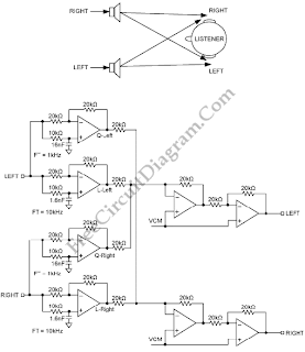
3D enhancement is needed to create a fully 3-dimensional sound for most stereo multimedia products. Usually, simple phase-delay circuits is used to produce a widening effect on the perceived sound field. However, there is transaural acoustic crosstalk effect. The following figure shows transaural acoustic crosstalk effect and schematic diagram of simple phase-delay circuits :


Transaural acoustic crosstalk effect is a condition where some sound from the right-hand stereo speaker reaching the left ear, and vice-versa.
This is an active circuit that uses first-order section to present a phase-shift filter with ft of 1kHz for the quadrature signal  and ft = 10kHz for the linear signal. It will produce 90° phase shift between the quadrature and linear signals over the audio bandwidth of 1kHz to 10kHz.

Video-Based Motion Sensor

The design is primarily based on an analog integrator circuit. The circuit integrates (i.e., sums) the input-voltage signal over a defined period of time. Based on an op-amp, the ideal circuit is shown in Figure 3. The factor –(1/RC) is constant, so the resulting output is inverted and proportional to the sum of the integrated values (i.e., proportional to the average of the signal in the integrated period of time). This is all it takes to “compress” the analog video signal.

Although it seems complicated at first sight, it should be fairly simple by now (see Figure 4). The integrator is implemented by a National Semiconductor LM6134B, a fast, rail-to-rail, single-power supply op-amp (U3). The output should then be quickly converted to digital because the input changes very fast. Analog Devices’s AD9280 ADC (U1) with 32 Msps was selected so a 50-ns capture could be performed. The AD9280 was configured for 1 to 2 V of input to use the internal 2-V reference. A 1-V reference was obtained with U3:D. To prepare the input for this range, the signal was inverted with the op-amp U3:A and clamped just less than 1 V with U3:B (see Figure 2). Just before the integration, the video was inverted under 1 V. The integrator was designed to output a 1-V signal when a ground-referenced, fully saturated video signal was input in 4.3-µs intervals. Note that the integrator is offset at 1 V. So, after signal integration, the ADC will receive a signal that is from 1 to 2 V as required. The integration capacitor C12 is a low-leakage metalized polyester film type. R8 is a metal film resistor, also a 1% part. To reset the integrator, a 74HC4066 analog switch (U4) is used. It is controlled by the ATmega88 through the INT_ENABLE signal. The video frame start is detected through the INT0 interrupt when the odd/even output of U2 changes. By using the odd/even output instead of the vertical synchronization output, the same pin can be used to determine if it is an even or odd frame. The video-line start is detected using the composite synchronization output of U2, which is connected to the AVR’s INT1 input.
The video output block performs the video highlighting. It is a transistor-based video amplifier that increases the gain when its enable signal is asserted low. Highlighting is used to show where a movement has occurred in the previous frame. It also gives you feedback on the blocks that will be ignored while executing the masking commands.
The only digital components in the design are the ATmega88 (U5), which has 8 KB of flash memory and 1 KB of RAM, a 20-MHz clock, and an RS-232-level converter (U6). The ATmega88, with its versatile instruction set, was key to developing this project. The generous 32 registers, bit-manipulation instructions, and word-pointer registers allowed the integration algorithm to fit in 4.7 µs, where the next sample should be captured. The software was developed in assembler to achieve the large optimizations required. I used AVR Studio 4 as the developing and testing environment.
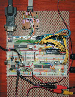
The circuit requires a regulated 5-V power supply for the analog and digital circuits. A single regulator can be used for both the analog and digital parts, provided that the signals are well filtered, and there is a single point of contact between the ground rails. Take a look at the motion-sensor prototype in Photo 2.

LCD thermometer for engine of vehicle with IC-L7136 circuit

Many car product in thermo sensor ,so i would like to show you the LCD thermo sensor which can modify for your car.


LCD car thermo circuit
When the thermometer is the IC thermo sensor (S8100) or diode (1S1588) is used as thermal sensors.
When using the IC thermo sensor, the thermometry to +100 ° C -40 ° C are possible.
Also, when using the diode, measured at 150 ° C from -20 ° C are possible. Both sensors are contained in the set.
This time I used the diode as a heat sensor to measure more than 100 ° C. ICL 7136 of Intersil (Harris) used for the thermometer and measure the voltage change minute by management before the temperature diodes.
The 3-1/2 digit LCD (SP521PR) applied to the screen. The most significant digit can display a “1″.
ICL7136 electricity consumption is very small and it is possible to run about 3 months with 9-V cell. The essential parts are contained in the set. The plastic casing and the cell is contained. But there is a cable connecting the sensor.

Automatic Intruder Burglar Alarm


This is a burglar alarm circuit written by Ron J. Its features include automatic Exit and Entry delays and a timed Bell/Siren Cut-Off. It’s designed to be used with the usual types of normally-closed input devices such as – magnetic reed contacts – micro switches – foil tape – and PIRs. But it can be Easily Modified to accept normally-open triggering devices – such as pressure mats.
Hot It works
This intruder burglar alarm is easy to use. First check that the building is secure and that the green LED is lit. Then move SW1 to the “set” position. The red LED will light. You now have about 30 seconds to leave the building. When you return and open the door – the Buzzer will sound. You then have about 30 seconds to move SW1 to the “off” position. If you fail to do so – the relay will energize and the Siren will sound.
While at least one of the switches in the normally-closed loop remains open – the Siren will continue to sound. However, about 15-minutes after the loop has been restored – the relay will de-energize – the Siren will Cut-Off – and the alarm will Reset. Of course, you can turn the Siren off at any time by moving SW1 to the “off” position.

Program for Deadlock detection algorithm

INPUT:
enter total no. of processes : 4
enter claim matrix :
0 1 0 0 1
0 0 1 0 1
0 0 0 0 1
1 0 1 0 1
enter allocation matrix :
1 0 1 1 0
1 1 0 0 0
0 0 0 1 0
0 0 0 0 0
enter resource vector :
2 1 1 2 1
enter the availability vector :
0 0 0 0 1
OUTPUT :
deadlock causing processes are : 1 2
#include<stdio.h>
#include<conio.h>
void main()
{
int found,flag,l,p[4][5],tp,c[4][5],i,j,k=1,m[5],r[5],a[5],temp[5],sum=0;
clrscr();
printf("enter total no of processes");
scanf("%d",&tp);
printf("enter clain matrix");
for(i=1;i<=4;i++)
for(j=1;j<=5;j++)
{
scanf("%d",&c[i][j]);
}
printf("enter allocation matrix");
for(i=1;i<=4;i++)
for(j=1;j<=5;j++)
{
scanf("%d",&p[i][j]);
}
printf("enter resource vector:\n");
for(i=1;i<=5;i++)
{
scanf("%d",&r[i]);
}
printf("enter availability vector:\n");
for(i=1;i<=5;i++)
{
scanf("%d",&a[i]);
temp[i]=a[i];
}
for(i=1;i<=4;i++)
{
sum=0;
for(j=1;j<=5;j++)
{
sum+=p[i][j];
}
if(sum==0)
{
m[k]=i;
k++;
}
}
for(i=1;i<=4;i++)
{
for(l=1;l<k;l++)
if(i!=m[l])
{
flag=1;
for(j=1;j<=5;j++)
if(c[i][j]>temp[j])
{
flag=0;
break;
}
}
if(flag==1)
{
m[k]=i;
k++;
for(j=1;j<=5;j++)
temp[j]+=p[i][j];
}
}
printf("deadlock causing processes are:");
for(j=1;j<=tp;j++)
{
found=0;
for(i=1;i<k;i++)
{
if(j==m[i])
found=1;
}
if(found==0)
printf("%d\t",j);
}
getch();
}

Types of Stepper Motors

Stepper motors come in two varieties: permanent magnet and variable reluctance. (The reader may be familiar with hybrid motors, which are indistinguishable from permanent magnet motors from the controller’s point of view.) Permanent magnet motors usually have two independent windings, with or without center taps. Center-tapped windings are used in uni polar permanent magnet motors. This can you see in the figure (1).

Bipolar permanent magnet and hybrid motors are constructed with a mechanism similar to that used in uni polar motor, except that the two windings are wired without center taps in the Figure 2. The motor itself is simpler, but the drive circuitry needed to reverse the polarity of each pair of motor poles is more complex.
Stepper motors come in a wide range of angular resolutions. The coarsest motors typically turn 90 degrees per step, whereas high resolution permanent-magnet motors can commonly handle 1.8 or even 0.72 degrees per step. With the appropriate controller, most permanent magnet and hybrid motors can be run in half steps, and some controllers can handle smaller fractional steps or micro steps. For permanent magnet and variable-reluctance stepper motors, when one winding of the motor is energized, the rotor (under no load) snaps to a fixed angle. It holds that angle until the torque exceeds the holding torque of the motor, at which point the rotor turns, trying to hold at each successive equilibrium point.

C program for Round Robin CPU Scheduling Algorithm

INPUT :
enter the process name : aaa
enter the processing time : 4
enter the process name : bbb
enter the processing time : 3
enter the process name : ccc
enter the processing time : 2
enter the process name : ddd
enter the processing time : 5
enter the process name : eee
enter the processing time : 1
OUTPUT :
p_name p_time w_time
aaa 4 9
bbb 3 3
ccc 2 6
ddd 5 10
eee 1 11
total waiting time : 39
average waiting time : 7.8000
1
2
3
4
5
6
7
8
9
10
11
12
13
14
15
16
17
18
19
20
21
22
23
24
25
26
27
28
29
30
31
32
33
34
35
36
37
38
39
40
41
42
43
44
45
46
47
48
49
50
51
52
53
54
55
56
57
58
59
60
61
62
63
64
65
66
67
68
69
#include<stdio.h>
#include<conio.h>
#include<process.h>
#include<string.h>
void main()
{
char p[10][5];
int et[10],wt[10],timer=3,count,pt[10],rt,i,j,totwt=0,t,n=5,found=0,m;
float avgwt;
clrscr();
for(i=0;i<n;i++)
{
printf("enter the process name : ");
scanf("%s",&p[i]);
printf("enter the processing time : ");
scanf("%d",&pt[i]);
}
m=n;
wt[0]=0;
i=0;
do
{
if(pt[i]>timer)
{
rt=pt[i]-timer;
strcpy(p[n],p[i]);
pt[n]=rt;
et[i]=timer;
n++;
}
else
{
et[i]=pt[i];
}
i++;
wt[i]=wt[i-1]+et[i-1];
}while(i<n);
 
count=0;
for(i=0;i<m;i++)
{
for(j=i+1;j<=n;j++)
{
if(strcmp(p[i],p[j])==0)
{
count++;
found=j;
}
}
 if(found!=0)
 {
 
 wt[i]=wt[found]-(count*timer);
 count=0;
 found=0;
 }
}
for(i=0;i<m;i++)
{
totwt+=wt[i];
}
avgwt=(float)totwt/m;
for(i=0;i<m;i++)
{
printf("\n%s\t%d\t%d",p[i],pt[i],wt[i]);
}
printf("\ntotal waiting time %d\n",totwt);
printf("total avgtime %f",avgwt);
}
INPUT :
enter the process name : aaa
enter the processing time : 4
enter the process name : bbb
enter the processing time : 3
enter the process name : ccc
enter the processing time : 2
enter the process name : ddd
enter the processing time : 5
enter the process name : eee
enter the processing time : 1
OUTPUT :
p_name p_time w_time
aaa 4 9
bbb 3 3
ccc 2 6
ddd 5 10
eee 1 11
total waiting time : 39
average waiting time : 7.8000

Java applet program that allows the user to draw lines, rectangles and ovals

1
2
3
4
5
6
7
8
9
10
11
12
13
14
15
16
17
18
19
20
import java.awt.*;
import java.applet.*;
/*
<applet code="Sujith" width=200 height=200>
</applet>
*/
public class Sujith extends Applet
{
 public void paint(Graphics g)
 {
  for(int i=0;i<=250;i++)
  {
   Color c1=new Color(35-i,55-i,110-i);
   g.setColor(c1);
   g.drawRect(250+i,250+i,100+i,100+i);
   g.drawOval(100+i,100+i,50+i,50+i);
   g.drawLine(50+i,20+i,10+i,10+i);
  }
 }
}
Output:
Java applet progrme for draw lines, circle, rectangle Java applet progrme for draw lines, circle, rectangle

Java applet program for handling mouse events

1
2
3
4
5
6
7
8
9
10
11
12
13
14
15
16
17
18
19
20
21
22
23
24
25
26
27
28
29
30
31
32
33
34
35
36
37
38
39
40
41
42
43
44
45
46
47
48
49
50
51
52
53
54
55
56
57
58
59
60
61
62
63
64
65
66
67
68
69
70
71
72
73
74
75
import java.awt.*;
import java.awt.event.*;
import java.applet.*;
/*
<applet code="Mouse" width=500 height=500>
</applet>
*/
public class Mouse extends Applet
implements MouseListener,MouseMotionListener
{
 int X=0,Y=20;
 String msg="MouseEvents";
 public void init()
 {
  addMouseListener(this);
  addMouseMotionListener(this);
  setBackground(Color.black);
  setForeground(Color.red);
 }
 public void mouseEntered(MouseEvent m)
 {
  setBackground(Color.magenta);
  showStatus("Mouse Entered");
  repaint();
 }
 public void mouseExited(MouseEvent m)
 {
  setBackground(Color.black);
  showStatus("Mouse Exited");
  repaint();
 }
 public void mousePressed(MouseEvent m)
 {
  X=10;
  Y=20;
  msg="NEC";
  setBackground(Color.green);
  repaint();
 }
 public void mouseReleased(MouseEvent m)
 {
  X=10;
  Y=20;
  msg="Engineering";
  setBackground(Color.blue);
  repaint();
 }
 public void mouseMoved(MouseEvent m)
 {
  X=m.getX();
  Y=m.getY();
  msg="College";
  setBackground(Color.white);
  showStatus("Mouse Moved");
  repaint();
 }
 public void mouseDragged(MouseEvent m)
 {
  msg="CSE";
  setBackground(Color.yellow);
  showStatus("Mouse Moved"+m.getX()+" "+m.getY());
  repaint();
 }
 public void mouseClicked(MouseEvent m)
 {
  msg="Students";
  setBackground(Color.pink);
  showStatus("Mouse Clicked");
  repaint();
 }
 public void paint(Graphics g)
 {
  g.drawString(msg,X,Y);
 }
}
Output:
Java mouse handling events Java mouse handling events

C program to find the Shortest path for a given graph

OUTPUT:
enter the cost matrix :
0 1 4 2 0
0 0 0 2 3
0 0 0 3 0
0 0 0 0 5
0 0 0 0 0
enter number of paths : 4
enter possible paths :
1 2 4 5 0
1 2 5 0 0
1 4 5 0 0
1 3 4 5 0
minimum cost : 4
minimum cost path :
1–>2–>5
1
2
3
4
5
6
7
8
9
10
11
12
13
14
15
16
17
18
19
20
21
22
23
24
25
26
27
28
29
30
31
32
33
34
35
36
37
38
39
40
41
42
43
44
45
46
47
48
49
#include<stdio.h>
#include<conio.h>
void main()
{
int path[5][5],i,j,min,a[5][5],p,st=1,ed=5,stp,edp,t[5],index;
clrscr();
printf("enter the cost matrix\n");
for(i=1;i<=5;i++)
for(j=1;j<=5;j++)
scanf("%d",&a[i][j]);
printf("enter  number of paths\n");
scanf("%d",&p);
printf("enter possible paths\n");
for(i=1;i<=p;i++)
for(j=1;j<=5;j++)
scanf("%d",&path[i][j]);
for(i=1;i<=p;i++)
{
t[i]=0;
stp=st;
for(j=1;j<=5;j++)
{
edp=path[i][j+1];
t[i]=t[i]+a[stp][edp];
if(edp==ed)
break;
else
stp=edp;
}
}
min=t[st];index=st;
for(i=1;i<=p;i++)
{
if(min>t[i])
{
min=t[i];
index=i;
}
}
printf("minimum cost %d",min);
printf("\n minimum cost path ");
for(i=1;i<=5;i++)
{
printf("--> %d",path[index][i]);
if(path[index][i]==ed)
break;
}
getch();
}
OUTPUT:
enter the cost matrix :
0 1 4 2 0
0 0 0 2 3
0 0 0 3 0
0 0 0 0 5
0 0 0 0 0
enter number of paths : 4
enter possible paths :
1 2 4 5 0
1 2 5 0 0
1 4 5 0 0
1 3 4 5 0
minimum cost : 4
minimum cost path :
1–>2–>5

C program for finding remainder

OUTPUT:
enter frame:
1 0 1 1 0 1 0 0
enter generator:
1 0 1 0
remainder is:
0 0 1 0
1
2
3
4
5
6
7
8
9
10
11
12
13
14
15
16
17
18
19
20
21
22
23
24
25
26
27
28
29
30
31
32
33
34
35
36
37
38
39
40
#include<stdio.h>
#include<conio.h>
void main()
{
 int  i,j,gen[4],rem[4],frl=8,genl=4,k,k1,fr[11];
 clrscr();
 printf("enter frame:");
 for(i=0;i<frl;i++)
{
scanf("%d",&fr[i]);
}
for(i=frl;i<11;i++)
{
fr[i]=0;
}
printf("enter generator:");
 for(i=0;i<4;i++)
 scanf("%d",&gen[i]);
  for(k=0;k<frl;k++)
  {
   if(fr[k]==1)
   {
   k1=k;
    for(i=0,j=k;i<genl;i++,j++)
    {
     rem[i]=fr[j]^gen[i];
    }
 
    for(i=0;i<genl;i++)
    {
   fr[k1]=rem[i];
     k1++;
    }
   }
    }
      printf("\nremainder is: ");
      for(i=0;i<4;i++)
     printf("%d",rem[i]);
     getch();
}
OUTPUT:
enter frame:
1 0 1 1 0 1 0 0
enter generator:
1 0 1 0
remainder is:
0 0 1 0

Java program for creating multiple threads

1
2
3
4
5
6
7
8
9
10
11
12
13
14
15
16
17
18
19
20
21
22
23
24
25
26
27
28
29
30
31
32
33
34
35
36
37
38
39
40
41
42
43
44
45
46
47
class NewThread implements Runnable
{
 String name;
 Thread t;
 NewThread(String threadname)
 {
  name=threadname;
  t=new Thread(this,name);
  System.out.println("New Thread:"+t);
  t.start();
 }
 public void run()
 {
  try
  {
   for(int i=5;i>0;i--)
   {
    System.out.println(name+ ":"+i);
    Thread.sleep(1000);
   }
  }
  catch(InterruptedException e)
  {
   System.out.println(name+" Interrupted");
  }
  System.out.println(name+" exiting");
 }
}
class MultiThreadDemo
{
 
public static void main(String[] args)
 {
  new NewThread("One");
  new NewThread("Two");
  new NewThread("Three");
  try
  {
   Thread.sleep(10000);
  }
  catch(InterruptedException e)
  {
   System.out.println("Main Thread Interrupted");
  }
  System.out.println("Main Thread Exiting");
 }
}
Output:
New Thread :Thread[One,5,main]
New Thread : Thread[Two,5,main]
One:5
Two:5
New Thread : Thread[Three,5,main]
Three:5
One:4
Three:4
Two:4
One:3
Three:3
Two:3
One:2
Three:2
Two:2
One:1
Three:1
Two:1
One exiting
Three exiting
Two exiting
Main Thread Exiting

Java program that finds the area of a circle using Client-Server network

1
2
3
4
5
6
7
8
9
10
11
12
13
14
15
16
17
18
19
20
21
22
23
24
25
26
27
28
29
30
31
32
33
34
35
36
37
38
39
40
41
42
43
44
import java.net.*;
import java.io.*;
public class  server
{
 public static void main(String args[]) throws Exception
 {
  ServerSocket ss=new ServerSocket(2000);
  Socket s=ss.accept();
  BufferedReader br=new BufferedReader(newInputStreamReader(s.getInputStream()));
  double rad,area;
  String result;
  rad=Double.parseDouble(br.readLine());
  System.out.println("From Client : "+rad);
  area=Math.PI*rad*rad;
  result="Area is "+area;
  PrintStream ps=new PrintStream(s.getOutputStream());
  ps.println(result);
  br.close();
  ps.close();
  s.close();
  ss.close();
 }
}
public class  client
{
 public static void main(String args[]) throws Exception
 {
 
  Socket s=new Socket("192.168.0.19",2000);
  BufferedReader br=new BufferedReader(new InputStreamReader(System.in));
  String rad;
  System.out.println("Enter radius of the circle ");
  rad=br.readLine();
  PrintStream ps=new PrintStream(s.getOutputStream());
  ps.println(rad);
  BufferedReader fs=newBufferedReader(new InputStreamReader(s.getInputStream()));
  String result=fs.readLine();
  System.out.println("From Server : "+result);
  br.close();
  fs.close();
  ps.close();
  s.close();
 }
}
Output:
Java client
Enter radius of the circle
10
From Server: Area is 314.1341345

Java program for implentation of consumer problem using inter thread communication

Write a Java program that correctly implements producer consumer problem using the concept of inter thread communication.
1
2
3
4
5
6
7
8
9
10
11
12
13
14
15
16
17
18
19
20
21
22
23
24
25
26
27
28
29
30
31
32
33
34
35
36
37
38
39
40
41
42
43
44
45
46
47
48
49
50
51
52
53
54
55
56
57
58
59
60
61
62
63
64
65
66
67
68
69
70
71
72
73
74
75
76
77
78
79
80
class Q
{
 int n;
 boolean valueSet=false;
 synchronized int get()
 {
  if(!valueSet)
  try
  {
   wait();
  }
  catch(InterruptedException e)
  {
   System.out.println("Interrupted Exception caught");
  }
  System.out.println("Got:"+n);
  valueSet=false;
  notify();
  return n;
 }
 synchronized void put(int n)
 {
  if(valueSet)
  try
  {
   wait();
  }
  catch(InterruptedException e)
  {
   System.out.println("Interrupted Exception caught");
  }
  this.n=n;
  valueSet=true;
  System.out.println("Put:"+n);
  notify();
 }
}
class Producer implements Runnable
{
 Q q;
 Producer(Q q)
 {
  this.q=q;
  new Thread(this,"Producer").start();
 }
 public void run()
 {
  int i=0;
  while(true)
  {
   q.put(i++);
  }
 }
}
class Consumer implements Runnable
{
 Q q;
 Consumer(Q q)
 {
  this.q=q;
  new Thread(this,"Consumer").start();
 }
 public void run()
 {
  while(true)
  {
   q.get();
  }
 }
}
class ProdCons
{
 public static void main(String[] args)
 {
  Q q=new Q();
  new Producer(q);
  new Consumer(q);
  System.out.println("Press Control-c to stop");
 }
}
Output:
Put:1
Got:1
Put:2
Got:2
Put:3
Got:3
Put:4
Got:4
Put:5
Got:5
Put:6
Got:6
Put:7
Got:7
Put:8
Got:8
Put:9
Got:9
Put:10
Got:10
Put:11
Got:11
Put:12
Got:12
Put:13
Got:13
Put:14
Got:14

Java program that illustrates how run time polymorphism is achieved

1
2
3
4
5
6
7
8
9
10
11
12
13
14
15
16
17
18
19
20
21
22
23
24
25
26
27
28
29
30
31
32
33
34
35
36
37
38
39
40
41
42
43
44
45
46
47
48
49
50
51
52
53
54
class figure
{
 double d1,d2;
 figure(double a,double b)
 {
  d1=a;
  d2=b;
 }
 double area()
 {
  System.out.println("Area of the figure");
  return 0;
 }
}
class rectangle extends figure
{
 rectangle(double a,double b)
 {
  super(a,b);
 }
 double area()
 {
  System.out.println("Area of rectangle");
  return d1*d2;
 }
}
class triangle extends figure
{
 triangle(double a,double b)
 {
  super(a,b);
 }
 double area()
 {
  System.out.println("Area of triangle");
  return d1*d2/2;
 }
}
class runpoly
{
 public static void main(String[] args)
 {
  figure f=new figure(45,6);
  rectangle r=new rectangle(10,30);
  triangle t=new triangle(10,20);
  figure a;
  a=f;
  System.out.println(a.area());
  a=r;
  System.out.println(a.area());
  a=t;
  System.out.println(a.area());
 }
}
Output:
Area of figure
0.0
Area of rectangle
300.0
Area of triangle
100.0

PCI Signal Descriptions

2 PCI Signal Descriptions
2.1 System Pins

CLK
Clock provides the timing reference for all transfers on the PCI bus. All PCI signals except reset and interrupts are sampled on the rising edge of the CLK signal. All bus timing specifications are defined relative to the rising edge. For most PCI systems the CLK signal operates at a maximum frequency of 33 MHz. To operate at 66MHz, both the PCI system and the PCI add-in board must be specifically designed to support the higher CLK frequency. A 66 MHz system will supply a 66 MHz CLK if the add-in board supports it, and supply a default 33 MHz CLK if the add-in board does not support the higher frequency. Likewise, if a system is capable of providing only a 33 MHz clock, then a 66 MHz add-in board must be able to operate using the lower frequency. The minimum frequency of the CLK signal is specified at 0 Hz permitting CLK to be “suspended” for power saving purposes.
Figure 1: Signals defined in the PCI standard.
RST#
Reset is driven active low to cause a hardware reset of a PCI device. The reset shall cause a PCI device’s configuration registers, state machines, and output signals to be placed in their initial state. RST# is asserted and deasserted asynchronously to the CLK signal. It will remain active for at least 100 microseconds after CLK becomes stable.

2.2 Address and Data Pins
AD[31:0]
Address and Data are multiplexed onto these pins. AD[31:0] transfers a 32-bit physical address during “address phases”, and transfers 32-bits of data information during “data phases”. An address phase occurs during the clock following a high to low transition on the FRAME# signal. A data phase occurs when both IRDY# and TRDY# are asserted low. During write transactions the initiator drives valid data on AD[31:0] during each cycle it drives IRDY# low. The target drives TRDY# low when it is able to accept the write data. When both IRDY# and TRDY# are low, the target captures the write data and the transaction is completed. For read transactions the opposite occurs. The target drives TRDY# low when valid data is driven on AD[31:0], and the initiator drives IRDY# low when it is able to accept the data. When both IRDY# and TRDY# are low, the initiator captures the data and the transaction is completed. Bit 31 is the most significant AD bit. Bit 0 is the least significant AD bit.

C/BE[3:0]#
Bus Command and Byte Enables are multiplexed onto these pins. During the address phase of a transaction these signals carry the bus command that defines the type of transfer to be performed. During the data phase of a transaction these signals carry byte enable information. C/BE[3]# is the byte enable for the most significant byte (AD[31:24]) and C/BE[0]# is the byte enable for the lease significant byte (AD[7:0]). The C/BE[3:0]# signals are driven only by the initiator and are actively driven through the all address and data phases of a transaction.
PAR
Parity is even parity over the AD[31:0] and C/BE[3:0]# signals. Even parity implies that there is an even number of ’1′s on the AD[31:0], C/BE[3:0]#, and PAR signals. The PAR signal has the same timings as the AD[31:0] signals, but is delayed by one cycle to allow more time to calculate valid parity.

2.3 Interface Control Pins
FRAME#
Cycle Frame is driven low by the initiator to signal the start of a new bus transaction. The address phase occurs during the first clock cycle after a high to low transition on the FRAME# signal. If the initiator intends to perform a transaction with only a single data phase, then it will return FRAME# back high after only one cycle. If multiple data phases are to be performed, the initiator will hold FRAME# low in all but the last data phase. The initiator signals its intent to perform a master initiated termination by driving FRAME# high during the last data phase of a transaction. During a target initiated termination the initiator will continue to drive FRAME# low through the end of the transaction.
IRDY#
Initiator Ready is driven low by the initiator as an indication it is ready to complete the current data phase of the transaction. During writes it indicates the initiator has placed valid data on AD[31:0]. During reads it indicates the initiator is ready to accept data on AD[31:0]. Once asserted, the initiator holds IRDY# low until TRDY# is driven low to complete the transfer, or the target uses the STOP# signal to terminate without performing the data transfer. IRDY# permits the initiator to insert wait states as needed to slow the data transfer.
TRDY#
Target Ready is driven low by the target as an indication it is read to complete the current data phase of the transaction. During writes it indicates the target is ready to accept data on AD[31:0]. During reads it indicates the target has placed valid data on the AD[31:0] signals. Once asserted, the target holds TRDY# low until IRDY# is driven low to complete the transfer. TRDY# permits the target to insert wait states as needed to slow the data transfer.
STOP#
Stop is driven low by the target to request the initiator terminate the current transaction. In the event that a target requires a long period of time to respond to a transaction, it may use the STOP# signal to suspend the transaction so the bus can be used to perform other transfers in the interim. When the target terminates a transaction without performing any data phases it is called a retry. If one or more data phases are completed before the target terminates the transaction, it is called a disconnect. A retry or disconnect signals the initiator that it must return at a later time to attempt performing the transaction again. In the event of a fatal error such as a hardware problem the target may use STOP# and DEVSEL# to signal an abnormal termination of the bus transfer called a target abort. The initiator can use the target abort to signal system software that a fatal error has been detected.
LOCK#
Lock may be asserted by an initiator to request exclusive access for performing multiple transactions with a target. It prevents other initiators from modifying the locked addresses until the agent initiating the lock can complete its transaction. Only specific regions (a minimum of 16 bytes) of the target’s addresses are locked for exclusive access. While LOCK# is asserted, other non-exclusive transactions may proceed with addresses that are not currently locked. But any non-exclusive accesses to the target’s locked address space will be denied via a retry operation. LOCK# is intended for use by bridge devices to prevent deadlocks.
IDSEL
Initialization Device Select is used as a chip select during PCI configuration read and write transactions. IDSEL is driven by the PCI system and is unique on a per slot basis. This allows the PCI configuration mechanism to individually address each PCI device in the system. A PCI device is selected by a configuration cycle only if IDSEL is high, AD[1:0] are “00″ (indicating a type 0 configuration cycle), and the command placed on the C/BE[3:0]# signals during the address phase is either a “configuration read” or “configuration write”. AD[10:8] may be used to select one of up to eight “functions” within the PCI device. AD[7:2] select individual configuration registers within a device and function.
DEVSEL#
Device Select is driven active low by a PCI target when it detects its address on the PCI bus. DEVSEL# may be driven one, two, or three clocks following the address phase. DEVSEL# must be asserted with or prior to the clock edge in which the TRDY# signal is asserted. Once DEVSEL# has been asserted, it cannot be deasserted until the last data phase has completed, or the target issues a target abort. If the initiator never receives an active DEVSEL# it terminates the transaction in what is termed a master abort.

2.4 Arbitration Pins (Initiator Only)
REQ#
Request is used by a PCI device to request use of the bus. Each PCI device has its own unique REQ# signal. The arbiter in the PCI system receives the REQ# signals from each device. It is important that this signal be tri-stated while RST# is asserted to prevent a system hang. This signal is implemented only be devices capable of being an initiator.
GNT#
Grant indicates that a PCI device’s request to use the bus has been granted. Each PCI device has its own unique GNT# signal from the PCI system arbiter. If a device’s GNT# signal is active during one clock cycle, then the device may begin a transaction in the following clock cycle by asserting the FRAME# signal. This signal is implemented only be devices capable of being an initiator.

2.5 Error Reporting Pins
PERR#
Parity Error is used for reporting data parity errors during all PCI transactions except a “Special Cycle”. PERR# is driven low two clock periods after the data phase with bad parity. It is driven low for a minimum of one clock period. PERR# is shared among all PCI devices and is driven with a tri-state driver. A pull-up resistor ensures the signal is sustained in an inactive state when no device is driving it. After being asserted low, PERR# must be driven high one clock before being tri-stated to restore the signal to its inactive state. This ensures the signal does not remain low in the following cycle because of a slow rise due to the pull-up.
SERR#
System Error is for reporting address parity errors, data parity errors during a Special Cycle, or any other fatal system error. SERR# is shared among all PCI devices and is driven only as an open drain signal (it is driven low or tri-stated by PCI devices, but never driven high). It is activated synchronously to CLK, but when released will float high asynchronously through a pull-up resistor.

2.6 Interrupt Pins
INTA#, INTB#, INTC#, INTD#
Interrupts are driven low by PCI devices to request attention from their device driver software. They are defined as “level sensitive” and are driven low as an open drain signal. Once asserted, the INTx# signals will continue to be asserted by the PCI device until the device driver software clears the pending request. A PCI device that contains only a single function shall use only INTA#. Multi-function devices (such as a combination LAN/modem add-in board) may use multiple INTx# lines. A single function device uses INTA#. A two function device uses INTA# and INTB#, etc. All PCI device drivers must be capable of sharing an interrupt level by chaining with other devices using the interrupt vector.

 
Design by Free WordPress Themes | Bloggerized by Lasantha - Premium Blogger Themes | cheap international calls