Audio level meter (vumeter)


This circuit uses just one IC and a very few number of external components. It displays the audio level in terms of 10 LEDs. The input voltage can vary from 12V to 20V, but suggested voltage is 12V.
The LM3915 is a monolithic integrated circuit that senses analog voltage levels and drives ten LEDs  providing a logarithmic 3 dB/step analog display. LED current drive is regulated and programmable, eliminating the need for current limiting resistors.

The IC contains an adjustable voltage reference and an accurate ten-step voltage divider. The high-impedance input buffer accepts signals down to ground and up to within 1.5V of the positive supply. Further, it needs no protection against inputs of 35V. The input buffer drives 10 individual comparators referenced to the precision divider. Accuracy is typically better than 1 dB.

Obstruction Detector With 12C508 IR


Description
This project is inspired by the DPRG IRPROX project. They have a pretty good PCB layout and idea. I would like to thank them for posting their project for all of us to see and learn from, I wouldn’t have started PIC programming without them, or at least not nearly as quickly come up to speed! The pinout on my board allows either a five-wire or a four-wire connection to be made the former uses a disable line if desired. You can also put in a resistor or use a trimpot to adjust range. The trimpot locations are very generic, most pots will fit. Be careful not to adjust pot to 0 ohms! The IR proximity detector works very well, even in a brightly lit “noisy” environment. Instead of modulating the IR LED for 600us and then looking for a detection, I now look for a detection after every on/off cycle of an IR LED and count the number of hits that I get. I also look during the ‘off’ cycle when none of the IR LEDs are on and count the number of false hits that I get there. If I get more good hits than false hits then I say its a true detection. I then increment a counter as a sort of timer, when it passes a certain threshold, I notify a hit. At this time I check to make sure that a minimum number of good hits has been attained. At the same time I keep track via another time-out counter of noise hits. When this counter passes a certain threshold it then removes any detection that has been set. I fiddled a lot with the various threshold values for minimum number of good hits, time-out values and divisors for updating the false hit counts, and finally settled on the ones that currently used. I’m calling it a success and moving on to other projects! The source code for the, uhm, DLC IR proximity detector can be downloaded below as well as the PDF documentation for this kit.

Proximity Detector Circuit Based 555 IR


Description Sometimes you want a simple solution to a problem and you don’t mind if your main controller has to do the work. This IRPD requires the main robot processor to choose which side to look at, and requires it to “debounce” the results for reliably operation. But, it still works really well without any complex program code.
The NAND gate is a standard 74LS00 that you can get anywhere – even Radio Shack, same with the 555, IR detector (RS Everlight or Sharp GP1U58Y) and IR LEDs can also be gotten at Radio Shack. Parts are easy to find and simple to connect. This does not require any fancy wiring or parts placement. Make sure that you use a .1uf bypass cap next to the 555 and next to the IR demodulator. Tweak the 2K pot until you have 38KHz, if you have a ‘scope, this is a 1/38,000 period, or about 26.3us. If you are using a Parallax Basic Stamp II for your robotic controller, you can feed the output of the 555 in an I/O port and measure the frequency very easily. The code to do this is below. It assumes that you are using port 7 as the 555 input port.
‘Basic Stamp II Freq Counter
O555    con        7
freq    var        word Loop:
count O555,100,freq
debug dec5 freq*10,cr
goto Loop
One of the nifty things that make the 555 circuit fun to use is that you can use it to do IR communications with other devices that read IR at 38KHz! If you run pin 4 of the 555 to a Stamp II port instead of just tying it high, you can use the serout Stamp II command to modulate the IR in such a fashion that other IR demodulator equiped devices can read it! I’ve done it, it works – Have fun.

High Voltage Generator/Solid State Tesla Coil


Parts
R1 27 Ohm 5W Resistor or 27 Ohm 10W Resistor
R2 240 Ohm 5W Resistor or 240 Ohm 10W Resistor
BR1 50 Volt, 6 Amp Bridge Rectifier
C1 8000uf, 35 Volt Capacitor
Q1, Q2 2N3055 NPN Power Transistor
T1 24V 5A Transformer (See “Notes”)
T2 TV Flyback Transformer (See “Notes”)
S1 115V 3A SPST Switch
MISC Case, Wire, Heatsinks, Line Cord
Notes
1. T2 is a high voltage flyback transformer salvaged from an old TV, or ordered from Fair Radio Sales (see Where To Get Parts). Look for the biggest, most intimidating transformer you can find. Old tube TV’s are a good place to look. The transformer should not have a rectifier built in.
2. You will need to rewind the transformer’s primary. First, remove the old primary, being careful not to damage the high voltage secondary. If the transformer is wound with all windings incased in plastic, use another transformer. Second, wind on 5 turns of 18 AWG wire, twist a loop (center tap), and then wind on 5 more turns. This becomes winding C-D. Now, wind on 2 turns of 22 AWG wire, twist a loop, and wind on 2 more turns. This becomes winding A-B.
3. Q1 and Q2 will run HOT if not used with a large heatsink. After the circuit has been running for a minute or two, you should still be able to put your finger on the transistors without being burnt. Also, R1 and R2 will run hot.
4. If you experience arcing on the exposed transformer leads, select a lower voltage for T1. If you are powering the circuit with a power supply (see Power Supply), just crank down the voltage.
5. For a real high voltage output, connect a voltage multiplier (from an old TV or computer monitor) to the output of T2.
6. If the circuit does not work, reverse connections A and B.
7. I finally got around to taking some pictures of the circuit in operation.

Several RC5 Infrared Transmitter Circuit

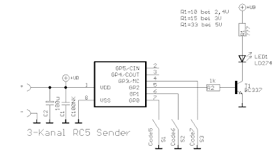
 1-channel transmitter with 16 selectable codes (PIC12C508)

RC5 is not suitable as a barrier to race out to whoever is the winner. Two or more RC5 channel interfere with each other and the protocol itself also takes time for the transfer. If more than one car with RC5 transmitter arrive close together, it can well be the first and the second triggers the stopwatch. IR does not pass through optical barriers through. Two car side by side is thus not before. Infrared is used in daylight outside, not really a good idea (the sun bothers!). With luck we can get a LOT still to reach 3m. Some wondered whether it was possible to hold down the button to send continuously or only one output to switch as long as a button is pressed. Is it possible that an output remains active for a certain time only? Yes, of course, is all that. This must DU EVEN each program change. I do not do that for you.
If the recipients are TSOP1836 TSOP1736 and specified. You need of course only one of them.
Which of the two is better? No idea.
After I had finished the RC5 tester, I have also done the same because a station building itself. The first attempt I have made with a PIC16F873. I used the PWM module to generate the frequency of 36kHz. Worked fine, but actually that was all much too large for a single channel. The 36kHz can also hold smaller produce PIC’s. These recipients are then a whole family of channels and come out.
On the function of the transmitter:
The PIC’s run in sleep mode until a key is pressed. The power consumption is then under 1uA. The circuit can then switch to the battery for a long time be without. Even with 3V button cells, the device should work very long.
When a button is pressed, the distance will be five RC5-wave pulse sent from the 50ms. That should suffice for the recipient to receive the code. After the PIC goes back into sleep mode. There is no repeat of the keys. This prevents the battery is discharged which when a key is pressed constantly unintentionally. All channels use the device code 29 to VCR, TV or CD player is not interfering.
! Attention!
In contrast to “normal” RC5 remotes do I change the toggle bit is not in any keystroke. Each key has a separate toggle. This is easier to force the receiver. It is therefore not possible, the receiver with a RC5 remote control to use! It is only with my stations.
For short distances, the LED directly from R2 (then 150 ohms or greater) to be connected and ground. The proposed power amplifier current is of about 100mA. Some of my remotes blow up to 250mA through the LED. For 5V could to increase the transmission power, a second LED in series with LED1. R1 is then 22 ohms.

About J0-3, the command code to be sent from 0-15 are set in binary code. Before each mission, the jumpers are queried. To send the code can then restart the PIC’s example by an additional circuit to be changed without it. As a clock for the PIC here I use the internal RC-oscillator. The is more precise than I had expected. Between 3V and 5V, it is no problem with the recipient. At 2.5 V (2xNiCd cell) it works but not always. Even at extreme temperatures, there could be problems. There must be a quartz oscillator to GP4 be connected fifth the number of adjustable codes unfortunately falls to four. Source code and internal file I need for rich to.
3-channel transmitter (PIC12C508)

 The transmitter sends the codes 5,6,7. GP4, 5 are open and are not used. Only GP0, 1,3 have internal pullups and can wake the PIC from sleep. the oscillator is the same as for the one-channel transmitter. GP4, 5 but are still free. So no problem.
5-channel transmitter (PIC16F84)

Although still at PORTB inputs are free only PORTB0, 4,5,6,7 used. The PIC can these inputs on an interrupt will wake from sleep only. Therefore, the maximum of five keys.PORTB4, 5,6,7 have internal pullups. The entrance to PORTB0 has no internal pullup resistor. Therefore, an external use. PORTB0 provides the code PORTB4 3 and 7, the codes just 4-7.
16-channel transmitter (PIC16F84)
 This receiver is equivalent to one-channel transmitter intended to be, but can be used with the other stations also. It is suitable when only a single device or set to only one function is to be executed, eg light on / off, central locking open / close. With the jumpers, the codes will be set 0-1.
1-channel receiver with 16 selectable codes (PIC12C508)

40 Watt Fluorescent Strobe Lamp Schematic


Part List:
C1/C2 2x Elko standing 1μF/16V
C3 1x
Ker. Scheibenkondens. 0.1 μF
C4 1x
HV-capacitor 1μF 350V axial
C5 1x
Elko stand. 470μF 25 V
C6 1x
Poly condensation. 0.068 μF 630V
D1-4 4x
Diode 1N4001
D5 1x
Diode 1N4007
L1 1x
Ignition coil (such as the normal speed camera strobe)
P1 1x
Poti 6mm 2.2 M
R1/R4 2x
Resistor 470R 1 / 4 W
R2/R9 2X
Resistor 47K 1 / 4 W
R3 1x
Resistor 10K 1 / 4 W
R5 1x
Resistor 270R 1 / 4 W
R6 1x
Resistor 1.2 K 1 / 4 W
R7 1x
Resistor 22K 1 / 4 W
R8 1x
Resistor 120K 1 / 4 W
Si1 1x
Backup medium time 160mA
Si2 1x
A pair of fuse holders
T1/T2 2x
Transistor BC557B
T3 1x
Transistor BC547B
Ta1 1x
Transformer 2x 2x 5V 500mA 5VA
TA2 1x
Trafo 1,2 VA 9Volt
Th1 1x
Thyristor 4A 400V T0220
TR1 1x
Triac 4A 400V T0220
The points J1 and J2 to connect with the two electrodes on one side of the fluorescent tube. The points J3 and J4 , connect with the electrodes on the other side. Now stretch a thin insulated!! Wire along the tube and glue it eg. Scotch tape firmly. This wire carries the ignition voltage of several thousand volts to the tube so that they ignite properly. This wire, connect one end with J7 on the board, while the other end must necessarily be isolated. This wire leads except the high voltage pulses that is also voltage. The points with J5 and J6 of the board is one, tube fitting, ballast clamped to (choke, there’s the light trading.) Finally there is the voltage at J8 and J9. Now it should somehow already shine or flash, with the potentiometer, the flash rate can be set.


The circuit works much like the original Strobos. except that a fluorescent tube is used. Thus, the fluorescent tube zündbereit remains constant, the two electrodes of the tube are continuously transformer Ta1 supplied with electricity. This current makes the two resistance wires of the glow tube in, so the mercury evaporates into the tube and the electron emission is simplified. Ta2 Returns on the rectifier “D1-D4 , the voltage of the multivibrator, the ignition frequency of the tube is responsible for. The speed of the AMV is with potentiometer P1 set. The pulse then passes through R3 to T3, is amplified there and controls the bias for the triac, the conducting of these alternates. If so, then the circuit through the tube and the ballast closes and the tube can light up. The pulses of T3 also enter via the capacitor C3 to the gate of the thyristor Th1. Simultaneously with the closing “of the circuit for the tube is Th1 -conductive and creates a short in the ignition coil current flow, which in turn generates a high voltage on the secondary. This voltage of several thousand volts is now operational on port J7 to a wire outside of the tube. The high voltage at the tube provides the necessary starting voltage so that it starts and can certainly light up until the thyristor Th1 locks again.

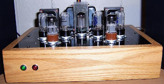
Hammond Transformers 6V6 Push-Pull Tube Amplifier


This 6V6 amp was built following the push-pull (PP) EL84 / 6V6 Dynaco A-410 output transformer schematic. There are a few minor deviations from the original schematics. Instead of Dynaco transformers, Hammond 1608A audio output transformers and a Hammond 272HX power transformer were used. The EL84 / 6V6 PP Dynaco A-410 output transformer schematic showed a 1000 ohm feedback resistor which resulted in bad amplifier oscillation. Feedback resistor Values between about 6 and 10 k-ohm worked well and I settled on 10k. A 5Y3 rectifier would have been to small for a stereo amp so a JJ GZ34 rectifier was used. It became necessary to put a 100 ohm resistor before the first power supply capacitor to bring down the B+ to about 325 volts as I was getting in excess of 345 volts (there is less voltage drop through a GZ34 versus a 5Y3).

Atmel at89c51 Office-Home Security System


Home security project
Securiy is a matter of great concern to all of us in this world. Normally there are four types of security threat to our property.
1 )Thief, an inturder.
2)Fire, so we use fire sensor.
3)Water spilage /over flow, so we use water sensor.
4) Gas leak , we use gas sensor, whenever there is security breach from one of above or any combination of above.
The project takes the following action
1) Sounds an ALARM to attract your home Security project
or public attention .
2) If the reset sw is not pressed within 30 seconds the projects takes further action,
3) It makes an emergency call to deliver an emergency message stored in speech IC.
4) It will make five attempts to call you before it checks the conditions again.


Atmel at89c51 Office-Home Security System
The project presented here is based on world’ s most powerful intel’ s mcs-51 family of microcontroller atmel at89c51. CIRCUIT EXPLANATION: This project is based on 8051 microcontroller.(IC2) IC3 and is used as buffer. IC4 is a one time programmable(otp) chip where messages are stored. This is 21 second speech ic where total of 12 messages can be recorded on eight different locations, but total duration should not be more than 21 seconds. Recorded messages can be played back by setting the trigger pin 10 & 11 to high, making these pin low will stop the message, Setting these pin high will repeatedly replay the same message. IC5 is an audio amplifire . Audio output from speech ic(IC4) pin no 7 cout is coupled to this ic on pin no 3 through VR2 volume control and C10. Amplified output from pin no 5 drives the speaker through capacitor C14. R14 and C13 corrects the tone. .C15 and C16 couples the audio message to telephone line. IC4 needs 3.3v operating voltage .R9 is a voltage dropping resistor, D7 is 3.3v zener diode and C7 is a filter capacitor. These components will always maintain the voltage to3.3v at pin 9,12 of IC4. capacitor C8 is a feed back capacitor.,C9 and R13 connected to pin no 7 of IC 4 are tone corrector.R12 along with the VR1 variable resistor performs the sampling rate adjustment. R10 and R11 connected to pin26 and pin 27 of the microcontroller are voltage dropping resistors. R15 and R16 connected to the base of transister Q1 and Q2 are voltage dropping resistors and drives transistors Q1 & Q2 when set to high logic by microcontroller. Q1 Drives the dial relay RL1and Q2 drives the off-hook relay.

12V Stroboscope 250-400V DC Circuit


The stoboscope tube needs about 250-400V DC to operate. This high voltage is generated using simple voltage step up circuit built from transistors Q1,Q2 and transformer T1. This circuit gives out about 230V AC voltage which is then rectified with rectifying bridge U1 (must have at least 400V voltage rating) and stored to the main capacitor C1.

I built my stroboscope from parts taken from old camera flash unit. This approach gave me nice flash tube with reflector, trigger transformer and some of the capacitors (for example C1). Other parts were the one luying around. I used some strange triac I found in my for the triggering circuit, but any triac which can handle at least 1A and 400V should do the job well.

12V Stroboscope 250-400V DC Circuit Component list
R1 1.2 kohm 1/2W
R2 1.2 kohm 1/2W
R3 120 ohm 2W
R4 10 kohm 1/2W
C1 100..150 uF 400V flash capacitor (from camera flash unit)
C2 4.7 uF 400V
C3 1 uF 400V
CZ 33 nF 400V
Q1 2N5983 NPN power transistors
Q2 2N5983 NPN power transistors
Q3 MAC216-4 Triac
TUBE Xenon flash tube (taken from camera flash unit)
T1 220V to 2x9V transformer, at least 10W power rating
T2 Xenon flash tube trigger transformer (from camera flash unit)
T3 Thyristor trigger transformer with good isolation
U1 Rectifier 1A 400V (can be build from four 1N4007 diodes)
S1 Switch one of three, at least 2A 400V rating

Output Relay Delay Audio Amplifier Circuit


Output Relay Delay Audio Amplifier Circuit
This is a simple circuit which I built to one of my audio amplifier projects to control the speaker output relay. The purpose of this circuit is to control the relay which turns on the speaker output relay in the audio amplifier. The idea of the circuit is wait around 5 seconds ofter the power up until the spakers are switched to the amplfier output to avoid annoying “thump” sound from the speakers. Another feeature of this circuit is that is disconnects the speaker immdiatly when the power in the amplifier is cut off, so avoinding sometimes nasty sounds when you turn the equipments off.
Output Relay Delay Audio Amplifier Circuit Component list
C1 100 uF 40V electrolytic
C2 100 uF 40V electrolytic
D1 1N4007
D2 1N4148
Q1 BC547
R1 33 kohm 0.25W
R2 2.2 kohm 0.25W
RELAY 24V DC relay, coil resistance >300 ohm
Circuit operation
Then power is applied to the power input of the circuit, the positive phase of AC voltage charges C1. Then C2 starts to charge slowly through R1. When the voltage in C2 rises, the emitter output voltage of Q1 rises tigether with voltage on C2. When the output voltage of Q2 is high enough (typically around 16..20V) the relay goes to on state and the relay witches connect the speakers to the amplifier output. It takes typically around 5 seconds after power up until the relay starts to condict (at absolute time depends on the size of C2, relay voltage and circuit input voltage).
When the power is switched off, C1 will loose it’s energu quite quicly. Also C2 will be charged quite quicly through R2. In less than 0.5 seconds the speakers are disconnected from the amplifier output.
Notes on the circuit
This circuit is not the most accurate and elegant design, but it has worked nicely in my small homebuilt PA amplifier. This circuit can be also used in many other applications where a turn on delay of few seconds is needed. The delay time can be increased by using bigger C2 and decreased by using a smaller C2 value. Note that the delay is not very accurate because of simplicity of this circuit and large tolerance of typical electrolytic capacitors (can be -20%..+50% in some capcitors).

10.58 to 10.74 MHz VFO Oscillator Circuit

Figure 1, below, shows the 10.58 to 10.74 MHz VFO oscillator circuit. Yes, this is the same circuit that was presented last time, but I’ve re-drawn it to show the Colpitts oscillator more clearly. “L” is approximately 1.5 uH; 19 turns in a T50-6 core (yellow). The value of C6 is found experimentally. I used 69 pF (a 47 pF and a 22 pF in parallel). More about this during check-out.


10.58 to 10.74 MHz VFO Oscillator Circuit
“L” and the V V C along with C6 make up the parallel-tuned circuit that determines the frequency of the VFO. The V V C is an MV2104. Capacitors marked with an asterisk must be silvered mica, COG, or NPO.

You might wonder how the component values for the resonant circuit are determined. Well, when Jupiter is aligned with Mars, and Mercury is on the cusp of a new moon, if the inductive reactance equals the capacitive reactance, then we have a resonant circuit. For any given frequency there are endless combinations of L and C that will produce a resonant circuit. Experience shows that variable capacitors and V V C’s in the 5 pF to 300 pF range are altogether practical. Combine this with the fact that a 1.5 uH coil and a 150 pF capacitor resonate near the frequency of interest, and you have the component values for this VFO’s resonant circuit. You can find formulas for figuring all this out in your Handbook, if you like to do arithmetic. The component values actually used in the circuit take into account “stray” inductance and capacitance that occurs in the real world. More about this during check-out.

RESONANT CIRCUITS are fascinating critters! While I’m NOT going to get into a theoretical discussion, there are some fundamental characteristics of resonant circuits that you (and I) should keep in mind when building VFO’s, filters, RF amplifiers, etc.

Two types of resonant circuits are commonly used: series resonant circuits and parallel resonant circuits, as shown below. Here are two important things to keep in mind: PARALLEL resonant circuits attenuate the flow of AC current at the resonant frequency (and pass all other frequencies); SERIES resonant circuits pass AC current at the resonant frequency (and attenuate all other frequencies).

RS-232 Reset for Microprocessor


RS-232 Reset for Microprocessor

Introduction
This circuit allows a remote microprocessor to be reset by a controlling host by sending a break signal over an RS-232 or RS-422 serial line. If the remote machine resets into a simple program loader program, it is possible for the host to halt and restart, or halt and reload/restart the remote machine’s program. This is an ideal way to develop software on older EPROM-based systems. Modern EEPROM/NVRAM systems use JTAG interfaces for similar results.
The remote processor runs its target code out of RAM, allowing the code to be updated easily. The circuit is usually used for developing code on a target processor, but it can also be used for permanent applications where the target program lives on a host system’s disk. This system was once used to load code into a microprocessor-based satellite receiving system in Hawaii from a host system in Colorado using an Internet-based remote serial communications program.
A program loader for the Z80 CPU is available below. The circuit has also been used with the Motorola 68HC11 EVB and the BUFFALO monitor program. See my Linux Cross Assemblers page for more info.

Theory
This circuit detects long duration zero level signals (breaks) on a NRZ (non return to zero) serial data line. Normal serial characters spend a short time in the zero state, and do not cause a reset. Break signals are a exception to this, they hold the line low for an extended period.
The 10K/1N4148 parts keep the 2.2uF capacitor charged up. Low input signals go through the 10K resistor and slowly pull the charge on the 2.2uF capacitor down. High input signals quickly recharge the capacitor through the 1N4148 diode. A break signal lasts long enough to discharge the 2.2uF capacitor to the point where the following gate changes state.
The 1N4148 on the right allows a manual break switch to be used on the target CPU, pressing such a switch does not short out the preceding 74HC14 gate.
This circuit could be built with just 2 schmidt trigger non inverting buffers, the 74HC14 was chosen because it is a common part. The parallel inverters are also optional, single inverters work fine.

Z80 Program Loader
Here is a Z80 assembly language program that functions as a bootstrap loader for use with the Microprocessor RS-232 Reset circuit. This code runs on an ancient SD systems SBC200 Z80 circuit board and can be made to work with other Z80 boards by changing the initialization and serial port functions.

Isolated RS422 Interface Circuit and Layout


 Isolated RS422 Interface Circuit
Figure 1 shows the circuit diagram of RS422 interface. Connector K1 is linked to the serial port of the PC, power to the PC side of the circuit is derived from the signal lines DTR and RTS. Positive supply is derived from RTS and negative supply from the DTR line. Optical isolation is achieved by optocouplers U1 and U2. Optocoupler  U1 provide TXD line isolation while optocoupler U2 provide RXD line isolation.

The other side of the isolator carries TTL levels. This side is powered by an unregulated dc supply between 9V and 12V ac/dc adapter. IC U5 provide 5V regulated output and ICs U3 & U4 provide the RS422 bus interface. The TXD and RXD lines status are provided by data indicating LEDs. The interface has been tested at the baud rate of 19.2k baud.

The connector K3 provide the RS422 bus signals plus the un-regulated dc supply output. An RJ45 connector can be used to provide the signals & power to the other end of the RS422 bus.
The PC RXD pin can only receive the data when the RS232 handshake lines are set accordingly,
RTS = 1  (at +ve supply level)
DTR = 0  (at -ve supply level)
For printing the pcb files on HP laser printer download the PCBs.zip file and run the Laser.bat file after extracting from the zip file.
Figure 2 & 3 shows the component layout of the RS422 single sided pcb and the track patterns respectively.


Component details of the project.
1 1 B1 BRIDGE 1A/100V (DIP TYPE)
2 3 C1,C2,C3 100nF CERAMIC
3 1 C4 10uF 16V
4 1 C5 470uF 25V
5 2 D1,D2 1N4148
6 2 D5,D3 LED RED 3mm
7 2 D4,D6 1N4003
8 1 K1 DB9 R/A PCB PLUG
9 1 K2 DC JACK SOCKET
10 1 K3 SIP CON 8 WAY
11 4 R1,R2,R5,R6 1K
12 1 R3 4K7
13 1 R4 470R
14 4 R7,R8,R9,R10 10R
15 2 R13,R11 120R
16 2 R14,R12 680R
17 1 U1 6N137
18 1 U2 CNY17-3
19 2 U3,U4 SN75176B, MAX485
20 1 U5 LM7805

0-1000 Volt Regulated High Voltage Power Supply IC 7805


1000 Volt DC to DC Regulator Circuit
Input voltage from high voltage DC DC converter is 12V AC at 800mA current and then converted to DC through a bridge rectifier Diode 1A. The voltage output of converter circuit can be adjusted in the range of 0-1000V DC. This high voltage DC DC converter uses the transformer as a base and several other active components include 555 timer IC, CMOS IC 4001, IC voltage regulator 7805, some NPN transistors and a pair of logic MOSFET IRF510 as a final amplifier.
The workings of high voltage DC to DC converter is the same principle as written in previous articles. The difference shown is this converter schematic is a high output voltage and can be arranged.
If a particular transformer mentioned in the schematic is not available, every transformer with primary specification 117V AC, 6.3V AC CT secondary to work. In this case, converter circuit operating at a sweet spot of the transformer, you may need to select a different drive frequency.
Be careful when handling high voltages! You are responsible for yourself.

AC to DC 90 Watt Switching Power Adaptor

AC to DC 90 Watt Switching Power Adaptor Circuit


AC to DC switching power adaptor circuit with maximum output power of 90W. Switching power supply is built using a high voltage power switching regulator IC MC33374 and some other additional components. The MC33374 IC is a monolithic high voltage power switching regulators that are specially designed to operate directly from a rectified AC line source, and in flyback converter applications.
The MC33374 switching power adaptor combines the required converter functions with a unique programmable state controller. At various variable AC inputs, it is capable of serving up to 6 A current at 15V output voltage. This switching power adaptor is capable of providing an output power in excess of 150W with a fixed AC input of 100V, 115V, or 230V, and in excess of 90 W with a variable AC input that ranges from 85V to 265V.

12V DC Motor Wind Turbine

12 volt Wind Turbine
It is possible to use a 12V DC motor (I assume its a car starter motor) as a wind turbine generator to provide energy conversion between the mechanical torque from the wind rotor turbines, (called the prime mover) and the connected 150V load. A gearless two or three bladed upwind wind turbine using a permanent magnet DC motor can be used to charge a battery for energy storage through a rectifier and a typical wind turbine configuration is given as:

Generator Configuration

However, using a low voltage DC motor as a wind turbine generator is not always a good idea for the following reasons.
  • The DC motor may not be rated for continuous use and overheat.
  • The motors maximum rotational speed may be exceeded on a gusty day resulting in bearing or mechanical failure of the armature, slip-rings and brushes.
  • A DC motor used as a generator does not provide a constant output voltage, when the shaft speed and the load current vary.
  • The output current may be high at a low 12V DC voltage requiring large diameter, low resistance cables between the generator and batteries.
  • The storage batteries and inverter electronics need to be as close as possible to the generator to reduce power loss in the cables.
  • The motors permanent magnets will attract ferromagnetic dust and debris.
  • Also relating to your situation, a special centre tapped “step-up” transformer is required to convert the 12V to 150V.
  • Then the alternative is to use a high voltage output wound rotor induction machine as a Wind Power Generator.
Regarding the electronics. You need to increase the voltage from 12 volts to 150 volts, therefore you will need a step-up transformer with a turns ratio of 1:12.5, The output power required on the secondary winding is: V x I = 150 x 1.5 = 225 VA minimum. Then the primary winding will be: 225 ÷ 12 = 18.75 amps. Therefore, you will require a transformer with a primary winding capable of handling 20 amps minimum as well as the switching transistors.
For a 50 or 60Hz output frequency the primary switching transistors (or Mosfets) need to switch at this frequency. A simple RC or RL oscillator can be constructed to produce the required sinusoidal waveform to convert the DC to an AC signal. It must have two complementary outputs “Q” and “not Q” to switch both halves of the transformer primary, You can use NAND gates or NOT gates (7400, 7404, 4069 etc) as an IC multivibrator but these will produce a square wave output signal.
The switching transistors can be any high current type capable of switching 20 amps at 40 volts minimum such as the 2N3771 or the TIP35C, or use lower current transistors in parallel but use a heatsink. Darlington transistors such as the NPN 2N6284 or the NPN SGSD100. One suggested (but not tested) switching circuit could be:
Possible Switching Circuit


Each half of the transformer primary is switched in turn to produce the secondary output. Because of the high current flow in the primary windings large diameter cables must be used. The pilot switching transistors can be any small 5-6 amp NPN transistor such as the TIP41, TIP121 etc. The diode is a normal 1-2 amp power diode.


Broadband Random Noise Generator


Broadband Random Noise Generator Circuit
This circuit is normally necessary in testing any sort of electronic methods for example filter, audio, or RF communication. The circuit introduced right here generates an RMS amplitude regulated noise source with selectable bandwidth. This circuit is work depending on op amp. This will be the figure with the circuit. Look at the schematic of Broadband Random Noise Generator Circuit above.
With 1 KHz to 5 MHz ten years ranges selectable bandwidth and 300mV RMS output, this noise generator is suitable for wide range of software. Noise is created by D1 that is AC coupled to A2, an amplifier with broadband acquire one hundred. The output of A2 is fed to a effortless selectable low-pass filter. The filter’s output is applied to LT1228 operational trans-conductance amplifier A3. A3’s output feeds current feedback amplifier LT1228 A4. A4’s output, which can be also the circuit’s output, is sampled by the A5-based gain manage configuration. This closes a gain manage loop to A3. A3’s ISET current controls gain, permitting overall output degree manage.

Two Speed Contactor DC Motor Controller Circuit


The simplest of all motor controllers (besides a straight on/off switch) is the contactor controller. I designed this contactor controller for use in my electric scooter project. It is based around three 12V relays, two 12V batteries, two switches and of course a motor. Having no silicon to “fry”, it is quite reliable and robust. A contactor controller works by rearranging the two (or more) supply batteries between series and parallel. This gives the motor a slow speed (batteries in parallel, current adds) and a fast speed (batteries in series, voltage adds). This assures that both batteries are discharged equally. When the circuit is “at rest”, the batteries are connected in parallel, which allows easy recharging.
Notes
1. S1 closes K3 and thus causes M1 to operate. S2 activates K1 and K2, reconfiguring the batteries for series operation and thus causes M1 to operate at “fast” speed.
2. B1 and B2 should be chosen based on the current requirements of M1. Often, sealed lead-acid type batteries are available at local suppliers for surprisingly low prices. These batteries are ideal for things such as scooters, go-karts, etc.
3. The relays are standard automotive type relays, available cheaply from any auto parts store.
4. Your motor will depend on your requirements. 12V motors will normally run fine at 24V, and vice versa.
5. You will notice that in series mode, all three relays only pull power from B2. This is because the relays have 12V coils, and it is impossible to switch the batteries from series to parallel and keep power to the coils at the same time. This does, however, mean that B2 is discharged slighty before B1. This should normally not be an issue unless the batteries are being drained completely “dead”. Draining a battery dead is not good for it in any situation, and should be avoided. If you wish, you can use a small 12V battery to run the relays separately.
6. You can add two more speeds to this controller using the schematic below. It connects at points A and B shown above on the controller schematic.

Parts

Part Total Qty. Description Substitutions
K1, K2, K3 3 12V 30A SPDT Relay (See Notes)
S1, S2 2 SPST Switch or Button
B1, B2 2 12V Battery (See Notes)
M1 1 12V or 24V Motor (See Notes)
MISC 1 Case, Wire, etc.

Counter Wall 7 Segment Circuit Diagram


This simple counter can be used to count pulses, as the basis for a customer counter (like you see at the doors of some stores), or for anything else that may be counted. The circuit accepts any TTL compatible logic signal, and can be expanded easily (see Notes).

Notes
1. All pulses to be counted are to be TTL compatible. They should not exeed 5V and not fall below ground.
2. You can add more digits by building a second (or third, or fourth, etc…) circuit and connecting the pin 11-6 junction of the 74LS90 and 74LS47 to pin 14 of the 74LS90 in the other circuit. You can keep expanding this way to as many digits as you want.
Part Total Qty. Description Substitutions
R1-R7 7 470 Ohm 1/4 Watt Resistor
U1 1 74LS90 TTL BCD Counter IC 7490,74HC90
U2 1 74LS47 TTL Seven Segment Display Driver IC 7447,74HC47
DISP1 1 Common Anode 7 Segment LED Display
MISC 1 Board, Sockets For ICs, Wire

Stepper Motor Pulse Generator with 555


The 555 Stepper Motor Pulse Generator kit will support you together with the pulse needed to drive your favorite DC Servo Motor application. This kit uses the well-known 555 timer IC for creating the Stepping Pulse.
Quick Overview
# Input : 5 to 12 VDC @ 25 mA
# TTL/CMOS interfaceable
# Jumper selectable two speed operation
# Onboard preset to vary the frequency
# Power-On LED indicator
# Terminal pins for easy interfacing of the kit
# Four mounting holes of 3.2 mm each
# PCB dimensions 39 mm x 37 mm

Lightning Detector Circuit


This Do-it-yourself lightning detector circuit can be a especially sensitive static electricity detector which can supply an early warning of approaching storms from inter-cloud discharge properly prior to an earth-to-sky return strike takes location. An aerial (antenna) formed of the brief duration of wire detects storms inside a two mile radius. The circuit emits an audible warning tone from a piezo buzzer, or flashes an LED for each discharge detected, providing you advance warning of impendig storms so that precautions may be observed.
The primary characteristic inside the lighting detector is the circuit’s ability to be set near to self-oscillation, with its leisure optimised via the bias resistor values demonstrated within the circuit diagram. The oscillator is dc coupled and feedback is routed through the collector of TR1 towards the base of TR2, whilst the overall loop acquire is set using the multiturn(12, eighteen or 22) preset VR1.
Lightning detector circuit establishing
To create the lightning sensor, change preset VR1 for oscillation by monitoring test point TP1, which must be at roughly 7volts peak-to-peak. Test level TP2 should be at +6V dc. Now readjust VR1 back again a bit to quit oscillation; use a screwdriver to touch the aerial-side of C1 a variety of occasions; the alarm ought to sound for one or two seconds then stop. If it continues, create a extremely tiny adjustment back again and recheck. The other technique is to electrostatically cost a plastic ruler after which draw your finger shut to discharge, about two meter away through the aerial.
Driven from a nine volts battery the lightning detector circuit consumes about 600 uA in standby. Powered continously it could supply a fantastic yr of uninterrupted monitoring. When sounding the alarm, the current will rise to 4mA based on the low current sounder WD1. A minimal three volts system is required for a great output level and it is going to create a “pinging” alarm to warn in real time of any electrostatic pulse activity.

CD4001 Simple Alarm Circuit For Motorcycle


Simple Alarm for motorcycle with a CD4001
This is a simple alarm circuit for a check with a 4001. You can use it to protect our home, motorcycle, car or any other application that comes to mind. In this circuit you will make a computer simulation with Livewire and then design the printed circuit Kicad.
OPERATION
SW1 is a normally closed switch when pressed triggers the flip-flop formed by the two NOR gates of the CD4001 and remains in that state for a time determined by the time constant of R5-C2. This time is the one who keeps the relay RL1 and operated by its two contacts that we investors will control two loads, for example a siren and a light or any other that we connect to P3 and P4.
After that time elapsed, the relay disconnects the circuit will soon be the alarm to be triggered again.
We can replace the switch Sw1 a PIR motion sensor, an infrared barrier, a smoke detector, gas detector, a magnetic sensor, a panic button or other device to act as a switch closed and opened fire at the alarm.
PRINTED CIRCUIT DESIGN
For the circuit we can only practical substitute for a preset R5 (RV1) so you can easily adjust the monitor while the charges.

Phase Delay Network for 3D Audio Enhancement

3D enhancement is needed to create a fully 3-dimensional sound for most stereo multimedia products. Usually, simple phase-delay circuits is used to produce a widening effect on the perceived sound field. However, there is transaural acoustic crosstalk effect. The following figure shows transaural acoustic crosstalk effect and schematic diagram of simple phase-delay circuits :

7 segment rolling display using PC

 It is very interesting and convenient to be able to control everything while sitting at your PC terminal. Here, a simple hardware circuit and software is used to interface a 7-segment based rolling display. The printer port of a PC provides a set of points with some acting as input lines and some others as output lines. Some lines are open collector type which can be used as input lines. The circuit given here can be used for interfacing with any type of PC�s printer port. The 25-pin parallel port connector at the back of a PC is a combination of three ports. The address varies from 378H-37AH. The 7 lines of port 378H (pins 2 through 8) are used in this circuit to output the code for segment display through IC1. The remaining one line of port 378H (pin 9) and four lines of port 37AH (pins 1, 14, 16, 17) are used to enable the display digits (one a time) through IC2. The bits D0, D1 and D3 of port 37AH connected to pins 1, 14 and 17 of �D� connector are inverted by the computer before application to the pins while data bit D2 is not inverted. Therefore to get a logic high at any of former three pins, we must send logic 0 output to the corresponding pin of port 37AH. Another important concept illustrated by the project is the time division multiplexing. Note that all the five 7-segment displays share a common data bus. The PC places the 7-segment code for the first digit/character on the data bus and enables only the first 7-segment display. After delay of a few milliseconds, the 7-segment code for the digit/character is replaced by that of the next charter/digit, but this time only second display digit is enabled. After the display of all characters/digits in this way, the cycle repeats itself over and over again. Because of this repetition at a fairly high rate, there is an illusion that all the digits/characters are continuously being displayed. DISP1 is to be physically placed as the least significant digit. IC1 (74LS244) is an octal buffer which is primarily used to increase the driving capability. It has two groups of four buffers with non-inverted tri-state outputs. The buffer is controlled by two active low enable lines. IC2 (75492) can drive a maximum of six 7-segment displays. (For driving up to seven common-cathode displays one may use ULN2003 described elsewhere in this section.) The program for rolling display is given in the listing DISP.C above. Whatever the message/characters to be displayed (here five characters have been displayed), these are separated and stored in an array. Then these are decoded. Decoding software is very simple. Just replace the desired character with the binary equivalent of the display code. The display code is a byte that has the appropriate bits turned on. For example, to display character �L�, the segments to be turned on are f, e and d. This is equivalent to 111000 binary or 38 hex. Please note that only limited characters can be formed using 7-segment display. Characters such as M, N and K cannot be formed properly.


PC based Frequency Meter

Here is a simple technique for measuring frequencies over quite a wide frequency range and with acceptable accuracy limits using a PC. It follows the basic technique of measuring low frequencies, i.e. at low frequency, period is measured for a complete wave and frequency is calculated from the measured time-period. Cascaded binary counters are used for converting the high-frequency signals into low-frequency signals. The parallel port of a computer is used for data input from binary counters. This data is used for measuring time and calculating the frequency of the signal. The block diagram shows the basic connections of the counters and parallel port pin numbers on 25-pin �D� connector of a PC (control register 379 Hex is used for input). External hardware is used only for converting the higher frequency signals into low frequency signals. Thus, the major role in frequency-measurement is played by the software. The PC generates a time-interrupt at a frequency of 18.21 Hz, i.e. after every 54.92 millisecond. Software uses this time-interrupt as a time-reference. The control register of the PC�s parallel port is read and the data is stored continuously in an array for approximately 54.9 ms using a loop. This stored data is then analysed bit-wise. Initially, the higher-order bit (MSB or the seventh-bit) of every array element is scanned for the presence of a complete square wave. If it is found, its time period is measured and if not then the second-highest order bit (sixth bit) is scanned. This operation is performed till the third bit and if no full square wave is still found, an error message is generated which indicates that either there is an error in reading or the frequency signal is lower than 19 Hz. Lower three bits of the control register are not used. When a wave is found, along with its time-period and frequency components, its measurement precision in percentage is also calculated and displayed. Number of data taken in 54.9 ms is also displayed. As stated above, the lower starting range is about 19 Hz. Data is read for approximately 54.9 ms. Thus, the lowest possible frequency that can be measured is 1/.0549 Hz. Lower range depends only on the sampling time and is practically fixed at 19 Hz (18.2 Hz, to be precise). Upper range depends on factors such as value of the MOD counter used and the operating frequency range of the counter IC. If MOD-N counter is used (where N is an integer), upper limit (UL) of frequency is given by UL=19xN5 Hz. Thus for MOD 16 counters UL@20 MHz, and for MOD 10 counters UL@1.9 MHz. Care should be taken to ensure that this upper limit is within the operating frequency range of counter IC used. Precision of measurement is a machine-dependent parameter. High-speed machines will have better precision compared to others. Basically, precision depends directly upon the number of data read in a standard time. Precision of measurement varies inversely as the value of MOD counter used. Precision is high when MOD 10 counters are used in place of MOD 16 counters, but this will restrict the upper limit of frequency measurement and vice-versa.


Simple Analog to Digital Converter

Normally analogue-to-digital con-verter (ADC) needs interfacing through a microprocessor to convert analogue data into digital format. This requires hardware and necessary software, resulting in increased complexity and hence the total cost.
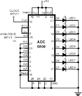
The circuit of A-to-D converter shown here is configured around ADC 0808, avoiding the use of a microprocessor. The ADC 0808 is an 8-bit A-to-D converter, having data lines D0-D7. It works on the principle of successive approximation. It has a total of eight analogue input channels, out of which any one can be selected using address lines A, B and C. Here, in this case, input channel IN0 is selected by grounding A, B and C address lines.
Usually the control signals EOC (end of conversion), SC (start conversion), ALE (address latch enable) and OE (output enable) are interfaced by means of a microprocessor. However, the circuit shown here is built to operate in its continuous mode without using any microprocessor. Therefore the input control signals ALE and OE, being active-high, are tied to Vcc (+5 volts). The input control signal SC, being active-low, initiates start of conversion at falling edge of the pulse, whereas the output signal EOC becomes high after completion of digitisation. This EOC output is coupled to SC input, where falling edge of EOC output acts as SC input to direct the ADC to start the conversion.
As the conversion starts, EOC signal goes high. At next clock pulse EOC output again goes low, and hence SC is enabled to start the next conversion. Thus, it provides continuous 8-bit digital output corresponding to instantaneous value of analogue input. The maximum level of analogue input voltage should be appropriately scaled down below positive reference (+5V) level.
The ADC 0808 IC requires clock signal of typically 550 kHz, which can be easily derived from an astable multivibrator constructed using 7404 inverter gates. In order to visualise the digital output, the row of eight LEDs (LED1 through LED8) have been used, wherein each LED is connected to respective data lines D0 through D7. Since ADC works in the continuous mode, it displays digital output as soon as analogue input is applied. The decimal equivalent digital output value D for a given analogue input voltage Vin can be calculated from the relationship

Control electrical appliances using PC

Here is a circuit for using the printer port of a PC, for control application using software and some interface hardware. The interface circuit along with the given software can be used with the printer port of any PC for controlling up to eight equipment .
The interface circuit shown in the figure is drawn for only one device, being controlled by D0 bit at pin 2 of the 25-pin parallel port. Identical circuits for the remaining data bits D1 through D7 (available at pins 3 through 9) have to be similarly wired. The use of opto-coupler ensures complete isolation of the PC from the relay driver circuitry.
Lots of ways to control the hardware can be implemented using software. In C/C++  one can use the outportb(portno,value) function where portno is the parallel port address (usually 378hex for LPT1) and 'value' is the data that is to be sent to the port. For a value=0 all the outputs (D0-D7) are off. For value=1 D0 is ON, value=2 D1 is ON, value=4, D2 is ON and so on. eg. If value=29(decimal) =   00011101(binary)  ->D0,D2,D3,D4 are ON and the rest are OFF.                       

Code Software in C :


/*program to control devices using PC parallel port
The devices are controlled by pressing the keys 1-8
that corresponds to each of the 8 possible devices
*/

#include<dos.h>
#include<stdio.h>
#include<conio.h>
#define PORT 0x378 /* This is the parallel port address */

main()
{
char val=0,key=0;
char str1[]="ON ";
char str2[]="OFF";
char *str;
clrscr();
printf("Press the approriate number key to turn on/off devices:\n\n");
printf("Here Device1 is connected to D0 of parallel port and so on\n\n");
printf("Press \"x\" to quit\n\n");
gotoxy(1,8);
printf("Device1:OFF Device2:OFF Device3:OFF Device4:OFF\n");
printf("Device5:OFF Device6:OFF Device7:OFF Device8:OFF");

while(key!='x' && key!='X')
{
gotoxy(1,12);
printf("Value in hex sent to the port:");
key=getch();
switch(key){

case '1':

    gotoxy(9,8);
    val=(val&0x01)?(val&(~0x01)):val|0x01;
    str=(val&0x01)?str1:str2;
    printf("%s",str);
    outportb(PORT,val);
    gotoxy(1,13);
    printf("%x",val);
    break;

case '2':

    gotoxy(21,8);
    val=(val&0x02)?(val&(~0x02)):val|0x02;
    str=(val&0x02)?str1:str2;
    printf("%s",str);
    outportb(PORT,val);
    gotoxy(1,13);
    printf("%x",val);
    break;

case '3':

    gotoxy(33,8);
    val=(val&0x04)?(val&(~0x04)):val|0x04;
    str=(val&0x04)?str1:str2;
    printf("%s",str);
    outportb(PORT,val);
    gotoxy(1,13);
    printf("%x",val);
    break;

case '4':

    gotoxy(45,8);
    val=(val&0x08)?(val&(~0x08)):val|0x08;
    str=(val&0x08)?str1:str2;
    printf("%s",str);
    outportb(PORT,val);
    gotoxy(1,13);
    printf("%x",val);
    break;

case '5':

    gotoxy(9,9);
    val=(val&0x10)?(val&(~0x10)):val|0x10;
    str=(val&0x10)?str1:str2;
    printf("%s",str);
    outportb(PORT,val);
    gotoxy(1,13);
    printf("%x",val);
    break;

case '6':

    gotoxy(21,9);
    val=(val&0x20)?(val&(~0x20)):val|0x20;
    str=(val&0x20)?str1:str2;
    printf("%s",str);
    outportb(PORT,val);
    gotoxy(1,13);
    printf("%x",val);
    break;

case '7':

    gotoxy(33,9);
    val=(val&0x40)?(val&(~0x40)):val|0x40;
    str=(val&0x40)?str1:str2;
    printf("%s",str);
    outportb(PORT,val);
    gotoxy(1,13);
    printf("%x",val);
    break;

case '8':
    gotoxy(45,9);
    val=(val&0x80)?(val&(~0x80)):val|0x80;
    str=(val&0x80)?str1:str2;
    printf("%s",str);
    outportb(PORT,val);
    gotoxy(1,13);
    printf("%x",(unsigned char)val);
    break;

    }

}


}

 
Design by Free WordPress Themes | Bloggerized by Lasantha - Premium Blogger Themes | cheap international calls