Low Power Under- and Over-Voltage Monitor

This voltage monitor has two  threshold, VTH for undervoltage and VTH’ for overvoltage. Using the component values shown in the schematic diagram below, this circuit give 6V for VTH and 15V for VTH1. Above 6V, the LED indicator of this voltage monitor  circuit will increase the flash rate until reach 15V.  This circuit will stop flashing at voltage below 6V and above 15 volts since there will be no current flowing through C1.  At threshold  boundary, the output of LM10 will saturate to negative below VTH and saturate to positive above VTH’.

To customize circuit we can select the resistors values according to chosen VTH and VTH’ using the following formula:
VTH=[R4(R1+R2)Vref]/[R1(R3+R4)];
VTH’=[R4(R1+R2)Vref]/[R1(R3+R4)-R3(R1+R2)]
Since the current consumption is very small (around 500uA), this voltage monitor will be suitable for various application  demanding low cost solution,  such as battery monitoring, small testing equipments, or power line indication.

5V FET Voltage Regulator

This voltage regulator circuit gives a stable 5V output from unregulated inputs (more than 5V). The stability of the output voltage is good enough, only change less than 0.1 volts when the load current changes about 60mA. Here is the schematic diagram of the circuit:

 The basic principle of the voltage regulation rely on the mechanism of keeping the the FET’s gate voltage at the cut-off point. The FET’s gate volage is the voltage across R2. At zero volt (when there is no current flowing through R2), the FET will be conducting, and a small current at FET (Tr1) will cause much larger current to flow through Tr3. This current will flow  through R2 and the gate voltage becomes negative. A some level the negative voltage at FET’s gate will cut-off the FETs current and  keep the output voltage stable

26V-to-5000V DC-DC Converter

This circuit can provide 5,000 VDC from 26 VDC. This circuit has ripple of under 0.01% due to Voltage-doubling capacitors. As sinusoidal oscillator, a 2N217 transistor is used. The diode and the capacitors at the output stage should be of high voltage type.  Here is the schematic diagram of the  circuit:

Transceiver Saver (Overvoltage Protector)

This is a transceiver saver circuit that protect  a transceiver device (applicable to other device as well)  from overvoltage of the power supply. This circuit is used to protect the device  by regulating the power supply,  avoiding damaging the device if overvoltage occurs.  If the transceiver transmits current of above 2A, a heatsink should be used for the transistor. The value of resistor must provide output of 12.6 V during normal operation, you can make trial and error through measurement when choosing this., you can start with value around 100R. It’s recommended to use a high wattage Zener diode. Here is the schematic diagram of the circuit:

Auto-Off 12V NiCd Battery Charger

NiCd/NiCad battery charger circuit is still needed since some application demanding high current is still rely on NiCd type, since this type is still superior in term of  high current output (low internal resistance) and low cost. This  battery charger circuit is used to charge 12V NiCd battery at  around 74 mA until battery is fully  charged. This circuit need  around 4 hours to fully recharge a totally empty/dead battery, depends on the battery capacity.  Here is the schematic diagram of the circuit


 This circuit is basically a current source with auto cut-off. The current regulation is done by maintaining a fix voltage across a 68R at the emitter of  2N2219 transistor. This voltage is stabilized by a 5.6V zener diode 1N752, which keep the voltage at 68R resistor at around 5V, giving a constant current of 74 mA.  The auto-off feature work by monitoring the output voltage (before the 1N4001 diode) relative to ground, as this voltage increases in accordance with the battery voltage which is being charged.  After the battery voltage reach the fully-charged level, the lower 1N752 zener diode will pass the current to activate the 2N222 transistor, which short the upper transistor’s base, turning off the charging process. To calibrate the shut off point, connect a 270 ohm / 2 Watt  resistor across the charge terminal and adjust the pot until the charging terminal voltage  show 15.5V level

Foldback Current Limited High Voltage Regulator

This circuit is high voltage regulator which has foldback current limiter protection. This circuit uses LM10 comparator with voltage reference, and this core integrated circuit is connected directly to high voltage circuitry. This high voltage direct connection is possible since the IC is inserted to a bias network and directly drop the applied voltage, so this IC is only suffering small voltage across its supply pins.

 The foldback current limiter is different with ordinary current limiter in the way the limiter responds to dynamic load. When we plot the regular current limiter, when the load draw a linearly increasing current, the plot of the current will be linear ramp which stops at a specified level determined by the limiter. A foldback current limiter will give same response until the current reach the maximum level, but will fold the current back to a much lower current level if the load try to further increase the current. This foldback action will prevent the final driver  transistor in the regulator from overheating

1 KW Power (Watt) Meter

This watt-meter circuit has measurement range up to 1-KW. This circuit can give the complete (X)(Y) function although uses only one transistor. Actually, this circuit is used for 117 Vac±50 Vac operation. For lower or lower voltage, this circuit can be modified easily. This circuit only measure power on negative cycles. The advantages of this circuit is this circuit does not need external power supply. This circuit measures true power that is delivered to the load. Here is the schematic diagram of the  circuit:


 At idle section, this circuit draw only 0.5W. This circuit has load current-sensing voltage of 10mV and load voltage loss of 0.01%. For linear loads, Rejection of reactive load currents is better than 100:1. When using a 50-μA meter movement, the nonlinearity of this circuit is about 1% full scale. Copper shunt can be used to give correct gain due to temperature

Simple Theremin with Inverter Gates

This simple but complete Theremin circuit is constructed using only two inverter chip plus one regulator IC. This Theremin circuit consist of five functional blocks: power supply regulator, hand controlled oscillator, null oscillator, mixer, and filter

The power supply regulator consist of LP2950 regulator IC, which stabilize the voltage from battery to 5V. You can use more popular 7805 IC for this, but since the power consumption of this Theremin circuit is very small, then you can use 78L05 which is smaller.  CR1 diode is used to protect from inappropriate battery polarity,  shorting the battery voltage together with R8 100 Ohm resistor which prevent the large current when the battery is installed in wrong direction. Although the inverter chip will work well for 9V battery, there is a benefit of using voltage regulation to regulate the battery voltage at lower voltage level, that the voltage will remain constant for until the end of battery life. This will avoid frequency drift of the Theremin’s null oscillator  which should be carefully adjusted to zero the output frequency, which can be affected by the supply  voltage.
Hand Controlled Oscillator
The hand proximity sensor is an oscillator which has antenna extension which shift the capacity coupling in the loop. This capacitance shift occur when we move our hand approaching the antenna. Since this change is very small in percentage, we need this oscillator to be high enough to produce notable frequency difference.  This oscillator block is built around U1A, U1B, and U1C. This oscillator give oscillation at around 73kHz. This frequency is not directly audible, we have to process this signal further to produce audible signal.
Null Oscillator
Null oscillator is employed to produce a constant frequency oscillation that will be used to produce differential frequency which is audible.  This oscillator block is built around U2A, U2B, and U2C. This null oscillator should be adjustable to set the null point where the Theremin should produce no oscillation at certain hand position.  At this point, the null oscillator should be adjusted to have  same frequency with the hand controlled oscillator since the audible Theremin output is the product of the difference between hand controlled and null oscillator frequencies.
Frequency Mixer (Differentiator)
The mixer is used to mix the signal from two oscillators, the hand controlled and the null oscillators. This mixer produce an output which contain many frequency components, not only the difference but also the original and the sum, since the amplifier U1F is basically a digital inverter which has non-linear transfer function. Fortunately, all the frequency components, except the difference, will be much higher than the needed signal and inaudible. This make it easy to remove by simple low pass filter to obtain only the differential frequency component.
Low Pass Filter
As stated before, we need to obtain only the audible frequency component by low-pass filtering. Although the high frequencies is inaudible, we still have to remove it since it can cause damage in audio power amplifier is the level is too high. It can distort the audible signal, and it can eat the electric power like ghost, frying your amplifier or at least make it overheated. This  Theremin circuit use simple low pass filter consist of C4, R5, and R7 for the passive stage, and C2 inside the inverter amp loop.

True Stereo Indicator Detects L-R Signal Difference

This true stereo indicator is different from what we usually find on FM radio receiver, which is usually a pilot tone detector. A stereo broadcast from FM radio station contain pilot tone, but a presence of pilot tone doesn’t necessarily a stereo broadcast signal since a mono FM transmitter ca broadcast pilot tone as well.  Since this circuit detect the difference between left and right channel, this circuit can detect a real stereophonic programs. When there is no difference between R and L input signals, the output A1 and output A2 is at the same potential. That will make a a virtual ground rail at half the supply voltage.

The A1 will supply a negative or positive voltage when A1 detects a difference between R and L input signals with respect to the virtual ground rail. The C4 will be charged via D2 an C3 via D1. The LED is turned on by the comparator A3/A4 via OR circuit D3/D4. The input signal level should be greater than 100mV to compensate for the drop across D2 or D1. P1 is used to adjust the sensitivity of stereo indicator.

53 dB Stereo Preamp for Tape or Phonographs

With the circuit shown in the following schematic diagram, both channels of this stereo preamp is constructed using  RCA CA3052 quad AC amplifier.  this pre-amplifier circuit is featured with tone control (bass – treble). Make a similar circuit to complete the other channel, since the circuit for left and right channel are similar. To be high-fidelity, total harmonic distortion should be kept minimum, this circuit gives less than 0.3% distortion level at  at 1-kHz testing signal with 1-V amplitude.  Gain or amplification at 1 kHz is 47 dB,  and the tone control will curve the response with 11.5-dB boost at 100 Hz and 10 kHz at maximum bass and treble boost.  For minimum bass and treble knob position,  the attenuation will be 10dB  at 100 Hz  and 9dB at 10kHz. This circuit is operated by a single ended supply for wider range environment. Inputs can be from tape recorders pickup or magnetic-cartridge phonographs.

Simple 9V Wireless Microphone FM Transmitter

This FM transmitter circuit can be used as a wireless microphone,  can be received by an ordinary 88- to 108-MHz FM broadcast receiver. For the power supply, this transmitter circuit is powered by a 9 V battery. To comply with the radiation limit of FCC rules, keep the antenna length under 12 inches. L1 is 6 turns of #24 wire wound around a pencil or a 1/4″ form, with turns spacing of 1 wire diameter. C6 is a gimmick capacitor which has value about 1 pF.

LM380, Simple 2 Watts Audio Amplifier

Small audio amplifier is useful for audio troubleshooting or simple audio projects. It should be a low cost and easy to build. Using integrated circuit for this purpose is the right choice. With LM380  audio amplifier integrated circuit, 2 Watts power can be delivered. For better thermal endurance, a large copper track can be printed in the board to provide heat sinking, this copper track should be soldered to pins 4, 3, 10, 5, 12 and 11.

Direct High Voltage DC Regulator

This regulator circuit stabilize the output voltage at 200V directly (without a transformer). Although the output voltage is high, this circuit only suffer a tension of the voltage drop (Vinput-Voutput), which is suffered mainly by the transistors. The op-amp suffers even less tension, since it regulate the applied voltage at their pins around the level of transistor’s bias voltage level.

Discrete Sliding Tone (Frequency Ramp) Doorbell

This doorbell circuit produces a low tone that will slide up to higher frequency. The equivalent total resistance connected between the base of Q1 and ground (Rbg) , and coupling capacitor  C1  determines the AF oscillator’s frequency. The resistance (Rbg) is equal to (R2+R1)R3. 

The R2 is used to set the initial bias condition, adjusted to produce a pleasant low starting frequency doorbell tone. D1 will start to conduct when Capacitor C3 charge through R6 until it reaches D1 bias  voltage level. Then the value of Rbg is paralleled by R4 and D1, and R5-D2-D3, and the values of diode’s equivalent resistance is gradually decreased as the C3 voltage ramp up.  This decreasing resistance value make the output tone slides up in frequency.  Two different diode path is provided to extend the linear area of diode conduction transition slope. With two path with different biases, after the single diode path has saturated, the second path provide further linear increase at higher voltage level.

LM3900 Audio Mixer

This audio mixer circuit doesn’t use a low impedance input to mix no ideal  sources, but use many amplifiers to provide  ideal sources before mixed through simple resistors. Ideal source means a sources with low impedances, make the interaction between signals in the output doesn’t affect the input.   Please note that this mixer circuit has high impedance output, so you’ll need an next processing equipment with appropriate  input specs. This audio mixer circuit is designed around an LM3900 quad op amp and combines 2 line and 2 mike inputs and sums them at the output terminal. To vary the gain (around +23 dB), we can change the R7 through R10.

Power Saver for Relays

Relays are normally operated at current level where it can initiate the mechanical metal contactors movement. After contacts has been established, the current level needed to keep the conductor plates stay attached is actually smaller than the current to initiate it. This power saver circuit seems to have opposite mechanism of surge protector. This circuit provide surge current to initiate mechanical movement, but after that, this circuit throttle the current to save the power, provide lower current level just to keep the contacts stay attached

The mechanism of this circuit is similar but done in opposite way with current surge protector. If we use a varistor with negative coefficient, here we use a kind of varistor but with positive coefficient, where the resistance increases as the temperature increase. This kind of varistor is actually an incandescent bulbs, two bulbs in parallel. At cold temperature, this bulbs has very low resistance, this make sure the relay will has sufficient power supply to initiate the mechanical movement of  its contactors. After the relay works, the rise of bulbs temperature will make the current decreased to a lower level, saving the power while maintaining the contactors stay attached. That’s all the mechanism of this power saver circuit.

TDA7056 3W BTL Mono Audio Power Amplifier


For mono output amplifier application,  TDA7056  IC can be your option. Compact but powerful, this integrated circuit is contained in a 9 pin medium power package. This device is designed for battery fed portable equipments such as mono recorders, radios and television. To attract the market, TDA7056 has many features such as low power consumption. For more reliable operation, TDA7056 also has short circuit proof and ESD (Electro Static Discharge) protected on all pins.  Designing application with this IC should be easy since no external components is needed. To make sure you’ll love this chip, this device also has no switch on/off clicks. Overall, TDA7056 has good stability.

Compressor Circuit with 570/571 Compandor IC


Compressor circuit provide high gain for low amplitude input and provide low gain for high amplitude input. This action, in effect, produce a nearly constant amplitude even though the input has very high dynamic range (very high amplitude variation from time to time). The action of compression like this is needed in some situation, such as in maximizing modulation depth in broadcasting, or sustaining electric guitar signal which has very high variation between the plucking time and fading out.  The following circuit has complementary input/output characteristic and unity gain at 0.775 VRMS input. Voltage gain through compressor is square root of 0.7/Vin. Vin is average input voltage. This circuit  uses Signetics dual channel compandor IC.  570 has lower inherent distortion and higher supply voltage range (6-24 V) than 571 (6-18 V).

Sound-Activated Lamp (Relay/Switch)


This simple circuit shown int the schematic diagram actives the switch using sound. We can use this circuit for various applications, such as automatic (sound-controlled) disco light or car’s LED light show.  The Q1 amplify the audio from mic. The R1 is used to adjust the peak of signal to greater than about 0.7 volts, act as sensitivity adjuster. A certain level, the signal coming from microphone, after amplification by Q1, will trigger the SCR and light lamp I1. If we change the lamp with a relay, then we can get a sound-activated relay/switch, which can be used to control more powerful / high wattage high voltage lamps. If we use a relay, place a 1N4007 diode in parallel with the relay coil to prevent the back-emf from  relay coil destroying the SCR.

Basic Complementary (Push-Pull) Power Amplifier Circuit


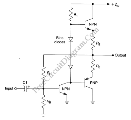
This amplifier circuit is very popular audio power amplifier circuit type. We call it a complementary since the final transistors is an NPN-PNP pair, each with the same characteristics. This circuit produce an AB class amplifier, since each transistor works in slightly more than half cycle of the signal. There is overlap area when both transistor conduct a current, and this area will be around its stationary current (when the input signal is zero). This circuit is also known as push-pull amplifier circuit since each transistor in the pair is working alternatively.

 
Design by Free WordPress Themes | Bloggerized by Lasantha - Premium Blogger Themes | cheap international calls